The introduction the Z68 Express Chipset has brought some nice new features to the GIGABYTE Z68X-UD7-B3 motherboard, including Smart Response, an SSD caching technology.
The Z68 Chipset and Smart Response
Introducing the GIGABYTE Z68X-UD7-B3
 Back in January, Intel released their P67 Express Chipset, which provided users with a great solution to build systems with powerful discreet graphics and Intel’s 2nd Generation Core architecture Sandy Bridge processors. The chipset also supported simple overclocking for high-end users. Due to the simplicity of overclocking, users on air cooling could easily reach speeds of up to 4.8 – 5 GHz. On the other hand Intel also released another very well known H67 Express Chipset. This category of motherboards were designed to use the processors built in integrated HD graphics to enhance video performance with systems running just integrated graphics. However, The H67 Express Chipset did not provide overclocking support for the CPU. Today, Intel is releasing the new Z68 Express Chipset, which combines the power of the H67 and P67 chipsets into one compact solution. There are two forms of Z68 based motherboards. One provides users with powerful dedicated graphics solutions with the support of the NF200 chip while also taking advantage of Intel’s new Smart Response SSD Caching technology. The other has display connectors on the rear of the motherboard, providing full support for the integrated graphics while having full CPU overclocking potential, and SSD caching called Smart Response. Today, we will be taking a look at GIGABYTE’s flagship high-end motherboard, the Z68X-UD7-B3, which follows the discreet graphics idea of the Z68 chipset. We will have a follow up review of GIGABYTE’s Z68X-UD3H-B3 motherboard which is using mainly the integrated graphics on the Sandy Bridge processors, but also comes with LucidLogix Virtu™ GPU Virtualization which allows switching between the integrated and dedicated graphics. This can help in more than one way, including lower power consumption when discreet graphics is not needed, or Intel’s Quick Sync media accelerator support which helps encode video quicker than ever.
In this review we’ll take a closer look at the differences on the GIGABYTE P67A-UD7-B3 and Z68X-UD7-B3 motherboard. The differences are minimal, but we’ll try to take a look at some of the main features that the Z68 chipset has to offer over the older P67 chipset. For those that are not yet familiar with the P67 chipset, we reviewed it in January. Please take a look at the GIGABYTE P67A-UD7 review which has an in-depth analysis of the P67 chipset on the Introduction page.
The GIGABYTE Z68X-UD7-B3 motherboard has an MSRP of $370, about $20 more than the P67A-UD7 when it was launched. This is expected because of the more expensive chipset and the extra features that come with the motherboard. It will be the users’ choice between the P67A-UD7-B3 or the Z68X-UD7-B3 motherboards depending on the features that they will need.
Intel smart response: SSD Caching Performance
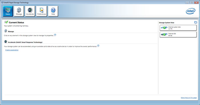
One of the most interesting features with the Z68 chipset is the Intel Smart Response, which is essentially the SSD caching. The idea is very much like Windows 7 ReadyBoost where using a flash storage device to cache contents. However, unlike ReadyBoost where flash drives are used as random disk, the SSD caching on the Z68 uses SSD to cache commonly used applications. This will result in faster application launch and system performance.
The SSD caching will not compete against real SSD in terms of performance but it will greatly enhance the system performance of a mechanical drive by adding a small size SSD. With commonly used data stored on the SSD, system will be more responsive and application will launch faster because SSD’s burst and sequential read performance is often two to five times faster than a mechanical drives.
To use SSD Cache, the following requirements must be met:
- 1 x SATA interface SSD drive capable of delivering read/write performance not slower than 100MB/s read and 150MB/s write.
- The minimum storage space needed for the SSD must be 20GB
- 1 x standard 7200RPM or 5400RPM HDD.
- A copy of Windows 7 operating system
Setting up the SSD Caching is also extremely easy thanks to the latest Intel Rapid Storage program. Simply follow the guideline below:
- Perform a full SECURE Erase of the SSD with application from the SSD vendor.
- Format the HDD into NTFS, follow by a full format of the HDD.
- Set the Intel SATA ports to RAID mode.
- Install OS onto the HDD.
- Install Intel RST 10.5, then reboot.
- Enter RST 10.5 control interface, and click on the Accelerate button.
- Select the SSD drive, the amount of space to be used as cache, the HDD volume to accelerate, and the acceleration mode*, then click on OK to proceed.
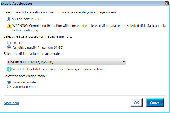
By default the a minimum of 18.6 GB of space on the SSD is needed to setup the SSD caching. Up to 64GB of space can be reserved for the cache. This is a good range as it offers enough space on the lower end for OS and 2-3 commonly used applications. Also, 64GB is a good number because if you can afford and SSD larger than 64GB, it would be much beneficial to use it as your primary drive for the best performance. After all, the data are still stored on the mechanical drive and if you ever need to access these data, you will not see the performance gain.
Intel offers two modes of caching mechanism: Enhanced and Maximized. While the read performance for both modes are roughly equal to the read performance of the SSD, the write performance for the Advanced Mode is a little slower than the slower of the two drives used (SSD or HDD). The write performance of the Maximized Mode on the other hand would be closer to the performance of the SSD. In addition, the Enhanced Mode offers stronger security as it utilize write-through strategy where data on the SSD and the hard disk are synchronized. In the event that the SSD is lost or damaged, no data is lost. The Maximized Mode utilizes write-back caching strategy where data are written to the disk in intervals. The risk here is that if the SSD failed or disconnected before the data has been written to the hard disk, the data will be lost.
Switching the modes can be as simple as click of a button
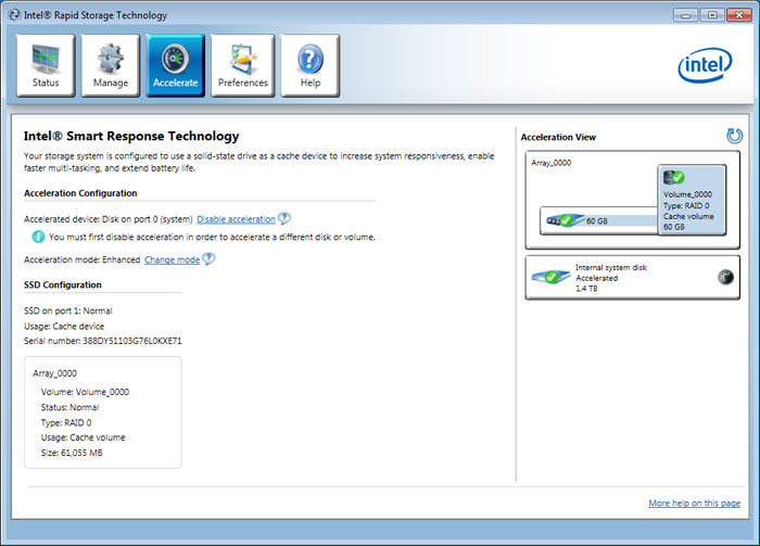
As we can see from the image above, once the SSD Caching has been enabled, a partition will be created on the hard drive with the same storage capacity as the SSD (or the size on the SSD reserved for caching). The software shows the hard drive and the SSD are configured as RAID 0.

Something neat about the way Intel handles the SSD cache is that when an SSD is set up as the cache drive, it will not show up under Windows Computer Management. This will prevent user from accidentally format the SSD.
At the moment, Intel Smart Response Technology (IST) only support 1 HDD and 1SSD or 1 RAID Partition + 1SSD. In addition, the average read and write speed of the SSD must be at least 50% faster than the hard drive in a single HDD+SSD combination, and at least 100% faster for RAID 0 to see the performance gain.
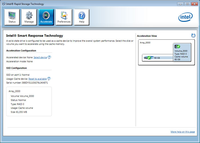
If you ever decide to stop using the SSD Caching, simply click on the “Reset to available” and the SSD can be used again as regular drive.
PCMark Vantage
PCMark Vantage is the latest system benchmark tool from Futuremark. The benchmark consists of tests such as application launches, file searches, web browsing, video playback, photo editing, and gaming.
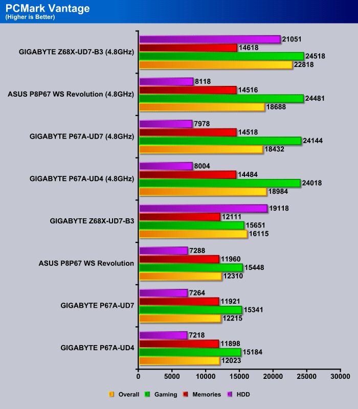
In the following tests have have went ahead and tested PCMark Vantage and paid close attention to the HDD Suite testing, and the overall PCMark Vantage Score. When comparing a standard HDD on the P67 motherboards compared to the Z68 where a HDD + SSD was used with Smart Response enabled, we can see a tremendous performance increase in the HDD Suite. The overall results also show on the PCMark Vantage overall scores. (Please check Testing & Methodology page for hard drive and SSD that we have used to measure performance in PCMark Vantage)
Windows Boot-up Performance
We went ahead and tested boot-up performance from the Windows loading screen to the Desktop screen of Windows. We closely measured these results and after 5 test runs we ruled out the first run and took the median of the 5 results.
| Microsoft Windows 7 Pro Booting Time | |
| Seagate Constellation ES.2 | 25.3 seconds |
| Seagate Constellation ES.2 + Intel 20GB Larson Creek SSD | 14.4 seconds |
From these two simple tests there is a clear comparison between a system that would be using just a SATA 7200RPM Hard Drive or the same Hard Drive with a 20GB Intel Larson Creek SSD. There is once again a noticeable performance increase making it possible for Windows 7 Pro to boot about 11 seconds faster than a system with just a Hard Drive. This performance increase happens after the system performs the same task twice in a row. This should also be noticed in other applications that might be taking advantage of the SSD Caching.
Special Features
Z68 Express Chipset New Features
- Quick Sync media accelerator support with with Intel’s second generation Core architecture. Most of Z68 board that have the integrated graphics support are enabled with LucidLogix Virtu™ GPU Virtualization technology, therefore, for gamers who require high-resolution gaming and they still able to enjoy the 3D graphic experience with 2nd generation Intel® Core™ processors. This is also a great salutation that GIGABYTE is offering to the high end users/gamers.
- Support for SSD caching technology called Smart Response. This option allows users to speed up their storage system by using a standard SATA Hard Drive with a standard SATA SSD. The SSD will work as a fast cache memory for the hard drive.
- GIGABTYE Touch BIOS™ (patent pending)
GIGABYTE Z68X-UD7-B3 Other Features
- Industry’s leading 24 phase power design for maximum power delivery.
- GIGABYTE Ultra Durable™ 3 design with 2x Copper PCB to provide the stability, reliability and longevity essential to meet the power needs of high-end processors and other components running today’s most demanding applications and games.
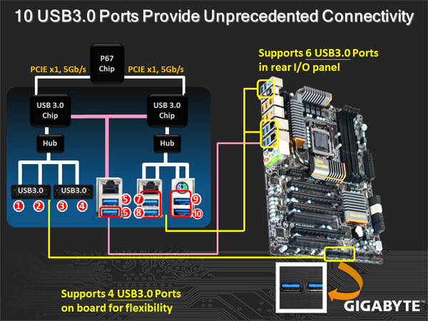
- Onboard 10 SuperSpeed USB 3.0 ports (total of 18 USB ports including USB 2.0) and 4 SATA 6Gbps to deliver impeccable data transfer speeds.
- CrossFireX™ and Nvidia® 3-Way SLI™ support for ultimate gaming experience.
- Matte Black color PCB offering a stylish new outlook that blends itself to decoration and case mods.
- Dual Gigabit LAN with Smart Dual LAN technology offering hassle free, zero downtime and high speed network connectivity
- Unique GIGABYTE 3x USB Power design with On/Off Charge USB ports to offer faster battery charging for iPhone, iPad and iPod devices.
- GIGABYTE patented DualBIOS™ technology delivering the highest level of failure protection.
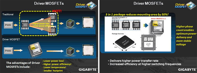
- Driver MOSFET Solution
- 3TB+ HDD Support
We categorized this board’s features for easier viewing.Though we previously saw similar implementation of intelligent energy savings and other PWM controllers, the VRD12 Design and the Driver MOSFETs add a bit more to the P67A lineup of motherboards by having something that we have not seen on previous GIGABYTE motherboards. The implementation of the 24 phase power, the VRD12 and Ultra Durable 3 design along with the new driver MOSFETs are mainly there for extreme overclockers and gamers.
The inclusion of 10x rear USB 3.0 5Gbps ports, 6x Internal SATA III 6Gbps ports, and of course the NF200 chipset for 3-way SLI and highe performance for each PCIE lane makes this motherboard outstanding. There is no manufacturer at the moment that we know of that would be able to squeeze a total of 10 USB 3.0 ports out of their motherboard. The UD7 is one of them.

 Like the pistons and cylinders of a car engine, the design of the motherboard Voltage Regulator Module (VRM), component quality and number of power phases greatly affects motherboard performance. GIGABYTE engineers were first to realize not only the importance of using the best quality components for this critical area, but also that with more power phases, there can be more power available to your CPU. GIGABYTE 6 series motherboards with their new redesigned VRM, promise to deliver first class system performance and power stability. With only the best quality components and unique design, incorporating Dual CPU Power and Power Phase Boost with Multi-gear Switching, your CPU can enjoy better power than what was available from previous motherboards.

GIGABYTE’s cutting edge 24 phase power VRM design utilizes the highest caliber components to provide unadulterated, smooth power to the CPU. The innovative 24 phase power VRM has been designed and engineered to deliver fast transient response times through quick and seamless power delivery during extensive CPU loading variations. In addition, heat from the VRM is effectively reduced by spreading the load between the 24 power phases, resulting in a cooler, more stable platform.

 Imagine a workstation class redundant (duplicated) power design on a desktop motherboard. GIGABYTE’s proprietary Dual CPU Power Technology allows CPU VRM power phases to split evenly into 2 sets of power engines that operate in tandem. This allows 1 set of power phases to rest while the other is active, as opposed to a traditional power design, where all the power phases are always active. As such GIGABYTE Dual CPU Power effectively halves the amount of work done by each set of power phases to significantly increase motherboard durability and reliability.


A traditional Voltage Regulator Module (VRM) consists of a Choke, Capacitors, MOSFETs and a Driver IC. By incorporating the MOSFETs and driver IC in accordance with the Intel® Driver-MOSFET specification, we can achieve higher power transfer and increased efficiency at higher switching frequencies to satisfy the growing power requirements of today’s processors. Driver-MOSFETs also help to reduce VRM real estate requirements in the CPU zone.


GIGABYTE DualBIOS™ is a patented technology that automatically recovers BIOS data when the main BIOS has crashed or failed. Featuring 2 physical BIOS ROMs integrated onboard, GIGABYTE DualBIOS™ allows quick and seamless recovery from BIOS damage or failure due to viruses or improper BIOS updating. In addition, GIGABYTE DualBIOS™ now supports booting from 3TB+ (terabytes) hard drives without the need for partitioning, and enables more data storage on a single hard drive.

The GIGABYTE Ultra Durable™ 3 design features twice the copper for both the power and ground layers of the PCB, dramatically lowering system temperature by efficiently spreading heat from critical areas of the motherboard (such as the CPU power zone) throughout the entire PCB. GIGABYTE’s Ultra Durable™ 3 also lowers the PCB impedance by 50%, which helps to reduce electrical waste and further lowers component temperatures. A 2x Copper layer design also provides improved signal quality and lower EMI (Electromagnetic Interference), providing better system stability and allowing for greater margins for overclocking…more

Note: Due to certain mobile phone limitations, users may need to connect the mobile phone to their PC before the PC enters S4/S5 mode to enable a quick charge from non On/Off Charge USB ports. Charging results may vary by model.


 GIGABYTE Ultra Durable™ 3 motherboards boast SuperSpeed USB 3.0 technology made possible through an additional onboard host controller. With superfast transfer rates of up to 5 Gbps, users are able to experience a theoretical 10x improvement over USB 2.0. Additionally, backwards compatibility with USB 2.0 assures users of long term use of their legacy USB 2.0 devices.
When GIGABYTE’s Turbo USB3.0 feature is enabled, it provides the fastest possible USB3.0 performance by allocating PCIe lanes to directly connect the CPU and USB 3.0 controller chip. This provides approximately 10% better performance than when it is disabled and USB 3.0 traffic is directed through the chipset.
Note: Turbo USB 3.0 utilizes 8 PCIe VGA lanes, so it is only possible to enable it with a single graphics card running at PCIe x8 on P67 chipset motherboards, or while using Intel® HD Graphics from the CPU (i.e. no VGA card) on H67 chipset motherboards. It is an option for high bandwidth users.


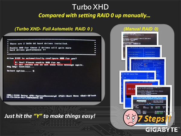
Turbo XHD function only enabled for the SATA controllers integrated in the Intel P67/H67 Chipset.


Featuring with two external SATA (Power eSATA) ports in the rear panel that provide smart setup and hot-plug functionality that allows easier data backup and content manipulation on external storage devices.


With 10 USB 3.0 and 6 SATA3 high speed storage connectors, the GA-P67A-UD7 allows for up to 10X faster USB 3.0 transfer speeds and 2X the throughput from existing SATA compatible drives.

GIGABYTE motherboards feature a high performance copper heat pipe with a sintered process to improve heat transfer between the heat source and the cooling fins of the heat sink. The heat sinks are designed for ultra efficient heat dissipation and are aided by the CPU fan blowing air down onto the CPU cooler.

Smart Dual LAN
GIGABYTE Smart Dual LAN technology features intelligent LAN port auto-switching between the 2 physical Gigabit LAN chips; offering hassle free, zero downtime, high speed network connectivity.


Dolby Home Theater® places listeners in the middle of the action, giving their PCs a powerful set of tools to deliver a cinema-style experience in vivid surround sound.
- Delivers vivid surround sound for music, movies, and games, using two to eight speakers or any set of headphones
- Designed to automatically deliver the best possible listening experience

Specifications

From what we understand, the Z68X-UD7-B3 will be the only motherboard to support 3-way SLI on GIGABYTE’s Z68 Express chipset motherboards due its use of the NF200 chip. The Z68X-UD5-B3 and UD4 motherboards will only have up to 2-way SLI support, meaning that those motherboards will not come with a 3-way SLI bridge or enough PCI-Express x16 slots for 3-way SLI support. The Z68X-UD3R-B3 will not have SLI support at all. For hardcore gamers, the UD7 will be the board of choice.
The UD7 also comes with 10x USB 3.0 ports, which means that almost all the USB connectors on the motherboard will be USB 3.0. USB 3.0 is backwards compatible with USB 2.0 devices, but provides 10x the performance of a USB 2.0 connector. Users will see an increased performance with even USB 2.0 devices that have a higher performance then what the interface is able to achieve, but will still be hindered by the limit of the USB 2.0 performance.
| Specification | GIGABYTE Z68X-UD7-B3 |
|---|---|
| CPU | Supports 2nd Generation Intel® Core™ processors in the LGA1155 package |
| Chipset | Intel® Z68 Express Chipset |
| Memory |
(Go to GIGABYTE’s website for the latest supported memory speeds and memory modules.) |
| Audio |
|
| LAN |
|
| Audio |
8-Channel Audio |
| Expansion Slots |
|
| Multi-Graphics Technology | Support for 2-Way/3-Way ATI CrossFireX™/NVIDIA SLI technology |
| Storage Interface | Chipset:
2 x Marvell 88SE9128 chips:
|
| USB | Chipset:
2 x Renesas D720200 chips and 2 x VLI VL810 hubs:
|
| IEEE 1394 | T.I. TSB43AB23 chip:
|
| Internal I/O Connectors |
|
| Back Panel Connectors |
|
| I/O Controller | iTE IT8728 chip |
| H/W Monitoring |
|
| BIOS |
|
| Unique Features |
|
| Bundle Software | Norton Internet Security (OEM version) |
| Operating System | Support for Microsoft® Windows® 7/Vista/XP |
| Form Factor | ATX Form Factor; 30.5cm x 24.4cm |
| Remark |
|
Software Overview

Here are some great applications that GIGABYTE includes with the Z68 motherboards. Most of these applications also come with other chipset motherboards, including the Intel P67, X58, P55, H57, H55, P45, P43 G41 series motherboards, and AMD 800 and 700 series motherboards. A nice addition to the software that GIGABYTE includes with their Z68 chipset motherboards is the Touch BIOS application. For more information about certain features, please make sure to check GIGABYTE’s website for updates.
The descriptions provided by GIGABYTE do an excellent job explaining what each of the application does.
 Dynamic Energy Saver™ 2
GIGABYTE Dynamic Energy Saver™ 2 incorporates a host of intelligent features that use a proprietary hardware and software design to considerably enhance PC system energy efficiency, Reduce power consumption and deliver optimized auto-phase-switching for the CPU, Memory, Chipset, VGA, HDD, and fans with a simple click of button.
|
||||||||||||
 Cloud OC
GIGABYTE Cloud OC is a free overclocking application that facilitates PC overclocking through any web browsing capable device such as a smart phone, iPad, iPhone, Netbooks or notebook PC. Being browser based it connects via wireless Internet, Bluetooth or through an Ethernet cable and its many functions are categorized into three tabs: Tuner, System Info and Control…more |
||||||||||||
 Hotkey OC
GIGABYTE Hotkey OC allows users to create and save various profiles that can be adopted for different benchmarks. Hotkey OC then allows users to jump between these profiles on the fly so that the best profile for each segment within the benchmark can be used to optimize scores and boost overall performance. So, for example, when running 3DMark 06 the 1st profile might be optimized for graphics and can be used for the first two graphics tests, then the next two tests can utilize the 2nd profile which might be optimized for CPU tests, and one could jump back to the 1st profile again for the final two graphics (shader) tests…more |
||||||||||||
|
Smart 6- A Smarter way for PC system Management
GIGABYTE Smart 6™ is designed with user-friendliness in mind, and offers a combination of 6 innovative software utilities that provide easier and smarter PC system management. Smart 6™ allows you to speed up system performance, reduce boot-up time, manage a secure platform and recover previous system settings easily with a click of the mouse button.
|
||||||||||||
 AutoGreen- Greening your PC via Bluetooth cellphone
AutoGreen technology can automatically save power for you simply by your bluetooth cell phone when you are away from your computer.
Note: GIGABYTE motherboards do not include a Bluetooth® receiver; the addition of a 3rd party Bluetooth receiver is required. |
||||||||||||
|
TouchBIOS TouchBIOS is a Windows based application that gives full control over the BIOS in real-time for the users that might not be used to the Traditional text based BIOS. This utility will allow users that just want to make quick changes to the BIOS with a graphical user interface right through Windows. TouchBIOS provides users with overclocking and boot options, while also having some nice tools like the Smart QuickBoost Utility, @BIOS Utility for updating the BIOS to the latest version, Integrated Hardware Menu, Power Management, Load BIOS Defaults, PC Status, and BIOS Password Locking. GIGABYTE Touch BIOS™fully supports any ‘Touch Screen’ monitor, which allows users to tweak their PC BIOS with the touch of a finger |
||||||||||||
 EasyTune6
GIGABYTE has completely redesigned EasyTune6 from the ground up to make it easier than ever to manage and monitor your hardware resources as well as tweak your system settings in order to achieve maximum system performance. Whether you are an overclocking enthusiast, or a computer novice, EasyTune6 provides the tools you need to quickly and effortlessly fine tune your system.
|


Unboxing the GIGABYTE Z68X-UD7-B3


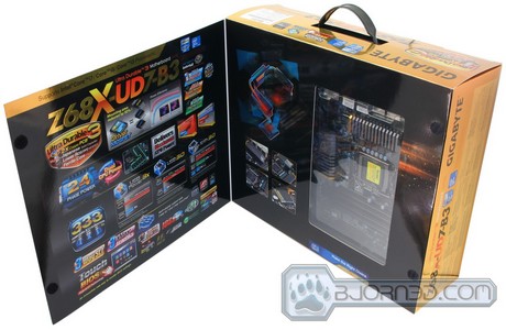
The new GIGABYTE Z68X-UD7-B3 motherboard’s box impressed us when we first saw it. Pictures don’t do the box justice, so we’ll describe it too. It has a nice black and golden scheme, and is extremely shiny. We can clearly see the new heatsink design that GIGABYTE uses on their P67 and Z68 motherboards. GIGABYTE also provides US and Canadian users with a 3 year warranty. This ensures that if there are any problems with the motherboard in the 3 years starting from the day of the purchase, buyers will have no problems returning the motherboard for a new one. On the front cover of the box we can also see the logo of the Ultra Durable 3 motherboard design, as well as that of the latest Intel Sandy Bridge architecture. The unlocked performance ribbon on the top along with the Delivers Maximum CPU Power means that the motherboard is be able to overclock the CPU to phenomenal frequencies. There is further information about Driver MOSFETs, 24 phase power, and all the high quality components this motherboard comes with.
The back of the box shows the features that we discussed on Page 2. Other features that are also described on the back of the motherboard include eSATAUSB Combo ports and Hardware Precision Over Voltage Control ICs.


The motherboard’s box has a flip cover, making it possible for the buyer to check out the motherboard before they commit to buying it. The same features, and a few new ones, are also explained in the inside flap of the front cover. On the right side under the front cover we can see what looks like Intel’s new CPU cooler for the Sandy Bridge processors. The diagram shows how the new heatsink design on the motherboard has excellent cooling potential with the combination of the Intel stock cooler. The air is blown towards the motherboard, spreading out on the sides of the socket, blowing through the motherboard’s heatsinks.


The way GIGABYTE designs their top of the line motherboards boxing seems to be the new standard for manufacturers like MSI, ECS, ASUS, etc. The first few times it felt as if the motherboard was not packaged properly and not protected enough without the anti-static bag, however, after reviewing several motherboards, we found that none of them ever had any problems. The boxing in the previous pictures seems to be just a very thin layer of cardboard. We had to take out the main black box from the shiny outer packaging in order to gain access to the motherboard and accessories. The black box opens up on the sides, where the carrying strap is. Once it is opened up, the inside of that box contains two more boxes: one which holds the motherboard, and the other which has all the accessories to the motherboard.
The cables and adapters are all packaged in bags, but we took all the accessories out of the bags for a better look. After several reviews and customer comments, GIGABYTE finally made the move to 100% black SATA cables. Their previous baby blue color scheme did not look very nice with the black and gold design on the motherboard.


The following accessories are provided with the GIGABYTE Z68X-UD7-B3 motherboard:
- Motherboard driver disk
- User’s Manual
- Quick Installation Guide
- Four SATA cables
- I/O Shield Plate
- Dual eSATA and Power bracket
- 2-Way SLI bridge connector
- 3-Way SLI bridge connector
- 2-port SATA power cable
- GIGABYTE sticker
- Dolby Home Theater sticker
Overview of the Z68X-UD7-B3


We first got a glance at GIGABYTE’s new high-end motherboard style back at IDF 2011. We got to try out the GIGABYTE P67A-UD7 motherboard back in January, and now we are presented with an almost identical board, the Z68X-UD7-B3. The black and gold scheme is only used on the high-end motherboards for GIGABYTE, while the old baby blue color scheme will still be used for the entry and mainstream level motherboards.
It seems like GIGABYTE continues to use their 2 oz copper design for motherboards, with only high quality Japanese capacitors and high quality Driver MOSFETs. They usually feel slightly heavier than other motherboards, and the PCB feels much sturdier. This showcases GIGABYTE’s Ultra Durable 3 design, which still amazes us 2 years after it was first announced. The Z68 LGA 1155 socket motherboards follow the P67 LGA 1155 architecture. We can see 4 DDR3 dual-channel slots, which are capable of 2200MHz frequencies, 2x PCI-Express x16 slots, and 2x PCI-Express x8 slots. The rest of the expansion slots consist of one PCI-E x4 slot, and two PCI x1 slots. It is a bit interesting that GIGABYTE decided to put two PCI slots on the Z68X-UD7-B3 motherboard, since most users will not be using PCI cards anymore. Some users still use Audio Cards that use PCI slots, though the 2nd PCI slot would remain unused unless there is a WiFi adapter or some other add-on card.


We do not like the way GIGABYTE organized the PCI-Express x16 slots on the P67A-UD7-B3 and Z68X-UD7-B3 motherboards. Instead of having a x16 x8 x16 PCI-Express spacing, they are still using the x16 x16 x8 design, which creates an area of low air circulation between the cards. ASUS was able to notice this early enough way back when PCI-Express came out, and it is really a big advantage over GIGABYTE’s Design. We have been directly in touch with GIGABYTE for the past year now regarding this problem, when we first reviewed the GIGABYTE X58A-UD7 motherboard, and even though we get replies that say that they will look into this and try to improve their products, we have not any indications that they are pursuing improvements to the PCI-E spacing. It is quite disappointing. While we did not see any improvements on the P67A-UD7-B3 motherboard, we were hoping that the Z68X-UD7-B3 would not have this problem, though we were disappointed.
If the user wants to keep the x16/x16 speeds on the PCI-Express lanes, they are forced to use both video cards right next to each other. This means the the first video card in the upper PCI-Express slot will absorb heat dissipated from the card below. Given the option of spreading out the video cards with more than just 1 slot in between, such a configuration provides more air circulation for the first card. The user can still use the first video card in the first PCI-Express x16 slot, and then use the 4th PCI-Express slot but only at x8 speeds for SLI.


For those who are wondering why some motherboards do not have a heatpipe heatsink design like the UD7 does, or why the new Sandy Bridge LGA1155 socket motherboards only have what seems to be a South Bridge heatsink and MOSFET heatsinks, this is actually not quite correct. The new layout of the P67 motherboards is a bit different from the previous motherboards that we reviewed. Just like the P67 express chipset, the Z68 is located right next to the expansion slots, where the South Bridge used to be on previous motherboards. The heatsink in the middle takes care of the NF200 chip, which is responsible for SLI support. Without the NF200 chip, 3-way SLI would not be possible. This is why the Z68X-UD7-B3 has a complete heatpipe heatsink design, whereas motherboards that don’t have the NF200 might lack the heatpipe heatsink.
We can also see that the heatsinks on the P67A-UD7 have been fully screwed on from the back, instead of using the old push-pin design. Screwing on the heatsink is much better than just using the push-pin design, because the heatsinks have a better and sturdier contact between the chips and other components on the motherboard.
As far as P67A-UD7-B3 and Z68X-UD7-B3 designs go, there is not a single design change on the motherboard. The only difference we could spot was the color of the pins for the I/O ports and different color coding for the top SATA ports on the motherboard.
A Closer Look at the Z68X-UD7-B3


Let’s start off on the left bottom side of the Z68X-UD7-B3. The first chip that we can see is the Texas Instrument IEEE 1394 controller. As the name says, the T.I. controller controls the IEEE 1394 ports, located right below the chip. This chip allows up to 3 IEEE 1394a ports (2 on the back panel, 1 via the IEEE 1394a bracket connected to the internal IEEE 1394a header). We can see a lot of high quality components on this motherboard, including the Japanese capacitors, and overall, the motherboard has a very clean design with the components.
In the second picture we see several smaller chips. The two chips towards the top of the second picture seem to be the NEC Renesas USB 3.0 controllers. The chip right on the bottom of the second picture is the 8 channel Realtek ALC889 Audio controller. The ALC889 codec is a Digital to Analog converter with a 108 dB Signal-to-Noise ratio playback quality. The audio on this motherboard is also Dolby certified, meaning that the overall quality of the audio should be decent, but of course it will not be as good as a dedicated audio card. We saw the same implementation of the ALC889 codec on the GIGABYTE X58A-UD7 and P67A-UD7-B3 motherboard. Towards the middle of the second picture, there are two more chips from Realtek. These are the RTL8111E LAN controllers. The GIGABYTE Z68X-UD7-B3 has a Smart Dual LAN technology which allows the 2nd chip to automatically kick in without requiring users to switch the network cable. This comes handy in case one of LAN chips encounters a hardware error. This means that the user will also stay connected without any downtime in case the first LAN chip encounters a hardware failure. With Teaming enabled on the chips, the user can get up to twice the performance of up to 2Gbps.


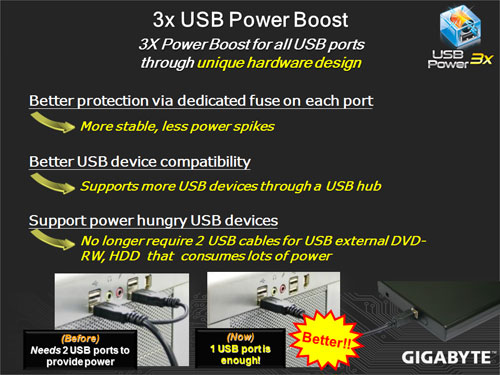
Towards the top left side of the motherboard, hiding behind the rear connectors and the MOSFET cooler, are two more chips from VLI, which also work with the USB 3.0 controllers. Looking at the same area from the other side shows several smaller components right next to the USB 3.0 and other connectors. These are USB port fuses which provide up to 4x lower resistance to ensure lower voltage drop. This allows for better USB 3.0 performance. With GIGABYTE USB 3.0 slots the user can get up to 2500mA of power through the ports making it possible to quickly charge iPads and other devices that require higher power output for charging. Usually there is a requirement to use two USB ports to power up, or to charge your devices than on a system that does not have 3x the voltage running through the USB ports.


If we take a look between the PCI-Express x16 and x8 slots, we can see several rectangular switches that split the 32 PCI-E 2.0 lanes between the four PCI-E slots we see on this motherboard. This means that when users are operating two video cards in the 1st and 3rd PCI-Express x16 slots, both slots will get x16 performance (x16/x16), but in a 3-way SLI or CrossfireX configuration, the 1st PCI-Express slot will stay x16, and the 3rd and fourth will become x8 (x16/x8/x8).
On the second picture we can see several connectors. The first connector on the left side is the IEEE 1394a Firewire connector. The two connectors to the right of that are fan connectors. It is sad to see that GIGABYTE is still using 3-pin fan headers instead of the 4-pin PWM fan headers, even though competitors use only 4-pin PWM fan connectors on their top of the line motherboards.
On the far right of the second picture, there are two larger connectors, which are actually connectors for a USB 3.0 extension kit to be placed in the front of the system. We are not quite sure why these connectors were placed on the bottom of the motherboard if they are most likely going to be used at the front of the computer. It would have been better to place these connectors to the right hand side of the motherboard, close to the 24-pin power connector, for easier access when a user connects such an extension unit. It is once again very interesting to see that GIGABYTE did not provide any such USB 3.0 extension units that users could attach to the front of the PC in a 3.5″ drive bay or a 5.25″ drive bay. We’ve seen ECS, MSI, and ASUS do that on their top of the line P67 motherboards. Users who wish to use this port for the GA-P67A-UD7 have to buy their own USB 3.0 extension unit.

Thankfully, GIGABYTE disposed of the Floppy and IDE connectors they had on the X58A-UD7 motherboard. Those connectors are from the dinosaur age, and many already use only SATA devices. After the two large USB 3.0 connectors, we can see yet another 3-pin fan header, and two front USB connectors that can easily be utilized by cases that already have USB 2.0 or USB 3.0 prepared on the top or front of the case. On the far right of the motherboard, we can see the front panel connectors for the Power and Reset switches, the Power and HDD LED connectors, and the Speaker connector. Moving a bit more to the right, we can see the Debug LEDs. These come in very handy when overclocking a system or in the event of a hardware failure. The Debug LEDs will provide the user with a code that they can look up in their user’s manual, and they will be able to easily understand where the problem is. Further up, right next to the Z68 chip’s heatsink, where the GIGABYTE logo is printed in gold, we can see two components that have a baby blue dot on them. These are the BIOS chips. The inclusion of two BIOS chips is a fail-safe measure. In the event of a BIOS failure on one chip, the system will automatically start using the second one so the first one can be reflashed. This saves the user from the hassle of an RMA, and can make overclocking more fun and less dangerous. Unfortunately, there is no option to actually switch between the BIOS chips as we could do on the ASUS Rampage III series motherboards.


On the second picture above, we can see that the Z68X-UD7-B3 comes with a Power Switch, a Reset Switch, and even a CMOS Switch, which can come very handy for people running their motherboards on a test bench. Additional 3-pin fan header is located right next to the 24-pin motherboard power connector.
Looking at the storage connectors, there are 4x SATA 3 ports and 4x SATA II ports. The 4x black SATA ports are the SATA II ports, and the far right gray ports are the SATA III ports. The white SATA III ports have eXtreme Hard Drive (X.H.D.) support, allowing for faster performance and easier RAID 0 configuration. Unfortunately, the P67A-UD7 motherboard only comes with 8x SATA ports, whereas the X58A-UD7 motherboard came with 10x SATA ports. This isn’t a large concern, however, because the competition seems to have a total of 8x SATA ports as well. This should be enough ports for an average and high-end user.
The Marvell 9128 chip controls the black SATA III ports, while the Intel Z68 chipset controls the white SATA III ports. The Marvell 9128 chip also controls the eSATA3 and USB in one ports.


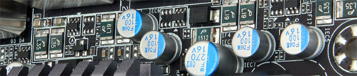
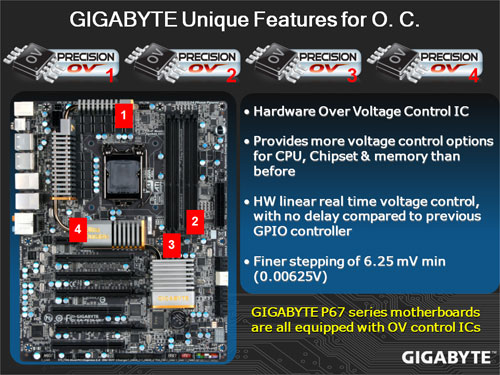
Finally, let’s take a look at the CPU socket and the surrounding components around it. From the first picture we see a PWM 4-pin CPU fan header and the VRD12 chip design right next to the MOSFET cooler. Overall we believe that the heatpipe heatsink design looks killer on this motherboard, especially with the gold colored sides. As mentioned before, right under the MOSFET coolers, there are 14 driver MOSFETs for lower power loss, higher power efficiency, lower temperatures, and a smaller footprint. From our tests by measuring the temperatures on the MOSFET heatsinks, it seems that the GIGABYTE motherboards run a tad bit cooler at the MOSFETs than the ASUS boards, though, this could actually also be a less heat conductivity from the thermal pads and the heatsink because ASUS usually has lower chipset temperatures. The heatsink to the far left corner of the motherboard has the number ‘7’ printed on it, representing the UD7 motherboard. Right behind the ‘7’ is the 8-pin CPU connector. We can also see a very clean design of the 24 phase power that GIGABYTE implemented on this motherboard. Though some may consider this excessive because even 16 phase power would be enough for extreme overclockers, the 24 phase power adds just a bit more stability and overall performance to the motherboard, while also ensuring that it runs cooler. Is this really necessary? Most likely not, and most users will probably not even stress the motherboard enough to fully utilize 12 phase power, though it can extend motherboard lifetimes due to less stress for each component. The last picture shows the LGA1155 socket, which is used by the latest Sandy Bridge processors. The GIGABYTE GA-P67A-UD4 and UD7 both have a very similar component design around the CPU socket. The capacitors right next to the socket are very close, making it very difficult to install water cooling blocks like the Heatkiller Rev 3.0 LGA 1156 cooler. Other air coolers with a larger base or extended heatpipe solutions might have a hard time fitting as well. The user needs to make sure their cooler is compatible with this motherboard.
Unfortunately, almost 90% of the problems we found on the P67A-UD7-B3 motherboard still exist on the Z68X-UD7-B3, and it seems as though GIGABYTE is being a bit lazy with fixing the issues. Another interesting part is that GIGABYTE does not have a hybrid solution for their higher end Z68 motherboards like ASUS does. For example, ASUS’ P8Z68-v Pro motherboard has support for SLI but also for integrated graphics as the Z68 chipset suggests. So while the P8P67 Pro motherboard was already a well built motherboard, the new P8Z68-V Pro has an additional HDMI output for the integrated graphics and support for discreet graphics like the GIGABYTE Z68X-UD3H-B3 motherboard. Since the Z68X-UD7-B3 does not have Virtu support unlike the UD3H, the UD7 will not have a display output by the I/O ports.
BIOS
Main Page


MB Intelligent Tweaker (M.I.T.)


It is interesting to see that while the BIOS for the GIGABYTE Z68X-UD7-B3 does not differ a lot from the P67A-UD7 or UD4, the sections that have options for different settings usually provide more options for the user. This is why the Z68X-UD7-B3 motherboard has more control over the settings in a system. The P67A-UD4 has all the necessary options that most users will require. For instance, the UD4 only has AUTO, Enabled and Disabled options for the Load-Line Calibration, while the UD7 has AUTO, Disable, Level 1, and Level 2 settings. To sum it up, the UD7 is a motherboard where everything can be fine tuned, while the UD4 has is a board for coarser adjustments. The UD4 and UD7 also allow for fine tuning each core’s multiplier, for the processor, especially with Turbo enabled.
Advanced BIOS Features


Integrated Peripherals, Power Management Setup & PC Heath Status


Overclocking

Those who really want to overclock their CPUs should pick the K series processor in combination with the Z68 chipset. Picking a non-K series processor will have limited control over multipliers and other overclocking features. Pairing the two will allow users to increase the core ratio, DDR3 ratio, power and current limit. We do not have the locked processor to test so we do not know how far it can be pushed. However, based on the Intel’s information, it appears that the Core i5 2500 can overclock up to 4.1GHz (41x100MHz) by raising the core ratio, while the 2500K and 2600K can achieve up to 5.7GHz (57x100MHz). This indicates that for locked processors, users can raise the core ratio up to 41x, while the unlocked can go up to 57x. However, each CPU has its own wall for multipliers. There is a 50% chance that a user will reach 4.5GHz speeds without reaching the multiplier wall, while there is a 20% chance for 4.7GHz, and a 10% chance for 4.8GHz to 5.0GHz. Finally, there is about a 2% chance the user will be able to overclock past 5.0GHz.
The nice thing with the Z68 chipset is that overclocking is possible even when integrated graphics is used. This is something that was limited on the H67 chipset and while the P67 had overclocking potential, it did not allow the users to use the integrated graphics. On the GIGABYTE Z68X-UD3H-B3 or the ASUS P8Z68-V Pro motherboard, it is possible to overclock the CPU multiplier and memory while also using integrated graphics. This is one nice addition to the small changes that happened from H67 and the P67 chipsets.
Intel’s Turbo also factors into overclocking because the processor will throttle to different clockspeeds depending on how many cores are active. We put together a chart that shows the Core i7 2600K processor running with Turbo off and with Hyper-Threading on. We have also left all , options enabled and downclocked when the CPU is at idle mode, but we turned off Intel Thermal Monitoring to prevent the processor from getting downclocked if critical temperatures are reached. However, this should not have affected our performance because we had a very powerful water cooling setup cooling the 2600K, but to get the best possible accurate results, we turned it off anyway.
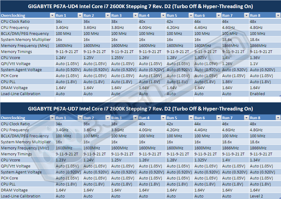
(While charts were taken from Previous P67A-UD7 and UD4 testing, the overclocking potential is still identical on the Z68 chipset according to our tests)
Immediately we can see that our charts stopped at 48x multiplier. This is due to the fact that each processor has its limitation — a wall — that it won’t go past. Though we were able to boot at 49X multiplier, the system would not be stable at all, even with high voltages. Here is an excerpt from an ASUS overclocking guide provided to us about the percentage of processors that overclock to a certain frequency from a total of 100 Sandy Bridge processors. Keep in mind that these tests were done without CPU PLL overvoltage turned on. With CPU PLL Overvoltage on both GIGABYTE and ASUS motherboards, the user can achieve over 5GHz speeds quite easily, though it prevents the user from using Sleep mode. If the user wants to use Sleep mode, they will have to disable CPU PLL Overvoltage.
Results are representative of 100 D2 CPUs that were binned and tested for stability under load; these results will most likely represent retail CPUs before the new CPU PLL Overvoltage setting was available in the BIOS. With the new CPU PLL Overvoltage, users can reach higher frequencies like 4.8GHz without having a lucky CPU.
1. Approximately 50% of CPUs can go up to 4.4-4.5 GHz
2. Approximately 40% of CPUs can go up to 4.6-4.7 GHz
3. Approximately 10% of CPUs can go up to 4.8-5 GHz (50+ multipliers are about 2% of this group)
Additionally it is recommended to keep 「C1E」and「EIST」option enabled for the best overclock scaling. This is different than previous Intel overclocking expectations where the best scaling was with disabled power states or power management options.”
However, by reaching the multiplier wall, the user is still not 100% finished with overclocking. It is still possible to overclock the BCLK as long as the hardware being controlled through the BCLK is not too sensitive to major changes in frequency. Since the BCLK is now controlling not only the CPU frequency, but also the Memory and PCI-E lanes, it is important to understand that there is only a slight change that can be done before the hardware will get unstable, especially PCI-E hardware like RAID cards and Video Cards.
For example, if the user finds the CPU ratio wall to be at 47x, but really wants to achieve 4.9GHz performance, it is still possible to bump up the BCLK to about 104.3 MHz. If we do the math, 47 x 104.3 = 4902 MHz or about 4.9 GHz.
Let’s take a look at the performance we were able to achieve with the Intel Core i7 2600K Sandy Bridge processor, and what temperatures were reached at certain voltages. The charts provided above show the voltages and settings used during each test. The screenshots below show the GIGABYTE P67A-UD7 motherboard used to overclock the 2600K processor. The Z68X-UD7-B3 has same overclocking potential according to our tests. Due to the fact that when we took these pictures, CPU-Z did not have a clear voltage reading from the motherboard, the VCore or Core Voltage is reported as 1.044V.
The temperature of the processor stays the same regardless of the motherboard, but for accurate settings during overclocking, please refer to the top charts.


Click Image For a Larger One
These are the results to the maximum frequencies we were able to achieve with the Core i7 2600K processor. According to the tests, temperatures were not a problem in reaching the limit of our processor. The actual limit we reached was the 48x multiplier wall. By enabling CPU PLL Overvoltage and using VDroop, we were able to achive a much higer overclock of up to 5.2GHz.
NOTE: Our water cooling loop is extremely quiet and does not get louder as load increases. We are running 3 fans that cool our radiators at 1400RPM, and the noise from the fans are completely inaudible at around half a meter away from the system. It would be difficult to reach such temperatures at low acoustic levels with air coolers. Our gratitude to AcousticPC.com for providing us with several parts to our complete water cooling loop.
Temperatures

The temperatures were recorded with CoreTemp while running LinX for a few hours during stability tests and double checking the results with OCCT for 20 minutes right after LinX finished its stress test. The processor was fully overclocked. The results were recorded carefully. After the results were recorded, we waited for 30 minutes before taking Idle temperature measurements. The results were as follows:
| Motherboard | Temperature (Idle / Load) |
|---|---|
| ASUS P8P67 WS Revolution B3 Rev | 39C/ 40C |
| ASUS P8P67 Pro |
37C / 38C |
| ASUS P8P67 Deluxe |
38C / 39C |
| GIGABYTE P67A-UD4-B3 |
38C / 40C |
| GIGABYTE P67A-UD7-B3 |
41C / 43C |
| GIGABYTE Z68X-UD7-B3 | 40C / 43C |
While the temperatures on the Z68X-UD7-B3 did not change that much, it is understandable because there is not much difference in architecture or design of the motherboard. GIGABYTE is reusing the same cooler as they used on the P67A-UD7-B3 motherboard as well as using the same components besides the different chipset.
Power Consumption

The power consumption was tested while running LinX for a few minutes at stock settings. The results were recorded carefully with a Kill-A-Watt power consumption measuring tool at the wall. After the results were recorded, we waited for yet another few minutes minutes before taking Idle power consumption measurements.
| Motherboard | Power Consumption (Idle / Load) | |
|---|---|---|
| ASUS P8P67 WS Revolution B3 Rev | 236W / 354W | |
| GIGABYTE P67A-UD4-B3 |
239W / 345W |
|
| GIGABYTE P67A-UD7-B3 |
245W / 355W |
|
| GIGABYTE Z68X-UD7-B3 |
249W / 365W |
There is a higher power consumption for the Z68X-UD7-B3 motherboard due to the fact that this system used an additional hard drive and SSD. It is not a big difference in power, but it is likely that the chipset itself is using a tad bit more power than the P67 Express chipset.
Testing & Methodology

(Water Cooling setup provided by AcousticPC.com)
We’ve expanded our testing suite considerably for the Z68 chipset, and will continue to use the same methods for most of the motherboards and CPU’s we test. In the interests of thoroughness and accurate results, we run each test at least three times, and some tests more than that. We average the total of all the tests from each benchmark then report the average here.
The OS we use is Windows 7 Pro 64bit with all patches and updates applied. We also use the latest drivers available for the motherboard and any devices attached to the computer. We do not disable background tasks or tweak the OS or system in any way. We turn off drive indexing and daily defragging. We also turn off Prefetch and Superfetch. This is not an attempt to produce bigger benchmark numbers. Drive indexing and defragging can interfere with testing and produce confusing numbers. If a test were to be run while a drive was being indexed or defragged, and then the same test was later run when these processes were off, the two results would be contradictory and erroneous. As we cannot control when defragging and indexing occur precisely enough to guarantee that they won’t interfere with testing, we opt to disable the features entirely.
Prefetch tries to predict what users will load the next time they boot the machine by caching the relevant files and storing them for later use. We want to learn how the program runs without any of the files being cached, and we disable it so that each test run we do not have to clear pre-fetch to get accurate numbers. Lastly we disable Superfetch. Superfetch loads often-used programs into the memory. It is one of the reasons that Windows occupies so much memory. Vista fills the memory in an attempt to predict what users will load. Having one test run with files cached, and another test run with the files un-cached would result in inaccurate numbers. Again, since we can’t control its timings so precisely, it we turn it off. Because these four features can potentially interfere with benchmarking, and and are out of our control, we disable them. We do not disable anything else.
Test Rig
| Test Rig | |
| Case | Silverstone Temjin TJ10 |
| CPU |
Intel Core i7 2600K @ 4.8 GHz |
| Motherboard |
GIGABYTE P67A-UD4 GIGABYTE P67A-UD7 ASUS P8P67 WS Revolution Motherboard GIGABYTE Z68X-UD7-B3 |
| Ram |
Patriot Gamer 2 16GB (4x4GB) DDR3-12800 1600MHz 9-9-9-24 Memory |
| CPU Cooler |
Heatblocker Rev 3.0 LGA 1156 CPU Waterblock Thermochill 240 Radiator |
| Hard Drives |
1x Constellation ES.2 3TB SATA Hard Drive 4x Seagate Cheetah 600GB 10K 6Gb/s Hard Drives 2x Western Digital RE3 1TB 7200RPM 3Gb/s Hard Drives |
| SSD |
1x Zalman SSD0128N1 128GB SandForce SSD 1x Intel SSD Larson Creek 20GB (Intel Smart Response w/ Seagate Constellation ES.2 3TB SATA Hard Drive) |
| Optical | ASUS DVD-Burner |
| GPU |
1x ASUS ENGTX580 Voltage Tweak Video Cards |
| Case Fans |
1x Quiet Zalman Shark’s Fin ZM-SF3 120mm Fan – Top 1x Silverstone 120mm fan – Front 1x Quiet Zalman ZM-F3 FDB 120mm Fan – Hard Drive Compartment |
| Additional Cards |
LSI 3ware SATA + SAS 9750-8i 6Gb/s RAID Card |
| PSU |
Sapphire PURE 1250W Modular Power Supply |
| Mouse | Razer Mamba |
| Keyboard | Logitech G15 |
Test Suite
We will use the following applications to test the performance of the Motherboard. Benchmarks
| Benchmarks |
|---|
| PcMark Vantage |
| Windows Boot Time |
| Cinebench R10 |
| Cinebench R11.5 |
| 3DMark 11 |
| 3DMark Vantage |
| Crysis Warhead |
| Just Cause 2 |
Cinebench R10 and R11.5

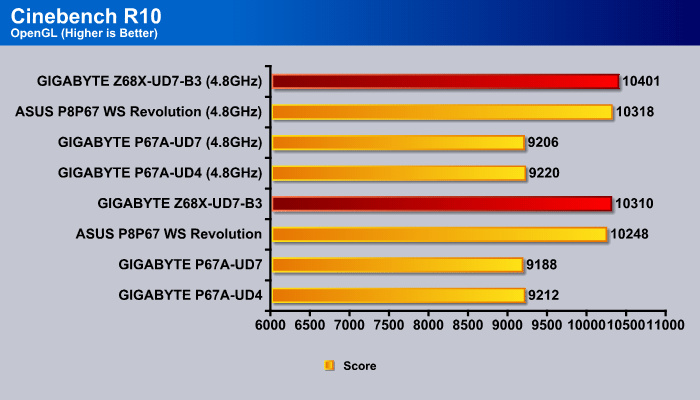
“CINEBENCH is a real-world test suite that assesses your computer’s performance capabilities. MAXON CINEBENCH is based on MAXON’s award-winning animation software, CINEMA 4D, which is used extensively by studios and production houses worldwide for 3D content creation. MAXON software has been used in blockbuster movies such as Spider-Man, Star Wars, The Chronicles of Narnia and many more. MAXON CINEBENCH runs several tests on your computer to measure the performance of the main processor and the graphics card under real world circumstances. The benchmark application makes use of up to 16 CPUs or CPU cores and is available for Windows (32-bit and 64-Bit) and Macintosh (PPC and Intel-based). The resulting values among different operating systems are 100% comparable and therefore very useful with regard to purchasing decision-making. It can also be used as a marketing tool for hardware vendors or simply to compare hardware among colleagues or friends.”
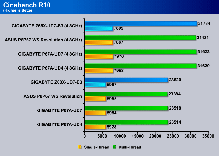
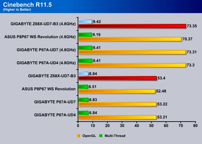
Same pattern can be seen in Cinebench R11.5.
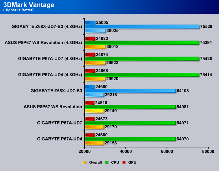
3DMark Vantage

For complete information on 3DMark Vantage Please follow this Link:
www.futuremark.com/benchmarks/3dmarkvantage/features/
The newest video benchmark from the gang at Futuremark. This utility is still a synthetic benchmark, but one that more closely reflects real world gaming performance. While it is not a perfect replacement for actual game benchmarks, it has its uses. We tested our cards at the ‘Performance’ setting.
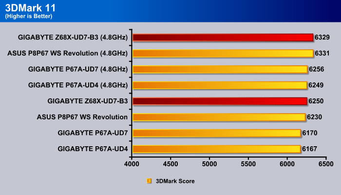
3DMark 11
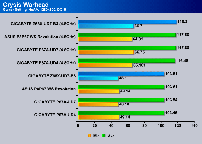
Crysis warhead

Crysis Warhead is the much anticipated standalone expansion to Crysis, featuring an updated CryENGINE™ 2 with better optimization. It was one of the most anticipated titles of 2008.
We ran Warhead using gamer’s setting at resolution of 1280×1024 and DirectX 10. We tested both no AA an 2x AA.
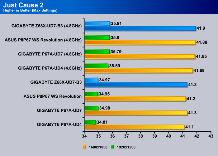
Just Cause 2

Conclusion
While the Z68X-UD7-B3 motherboard did not have too many big improvements over the previous P67A-UD7-B3 motherboard besides the new chipset and its features, it is the only motherboard on the market at the launch that has a NF200 chip and 3-way SLI and CrossFireX support. It is also a motherboard that has 8 USB 3.0 connectors, which is quite phenomenal compared to other Z68 motherboards on the market. So as far as the Z68X-UD7-B3 motherboard goes, it is one serious gaming and high-performance motherboard for users that can afford it at a high price of $370.
We really enjoyed the addition of Intel Smart Response SSD Caching technology, which proved to show a significant improvement in data loading performance and access times. This is definitely a feature a gamer or other high-performance user should look, into since it can provide significant performance increase in productivity and hard drive intensive applications. This is a prefect option for those that want high capacity, but also some of the performance that an SSD would provide.
The TouchBIOS feature that GIGABYTE is adding to their Z68 motherboards is a nice feature for those that are afraid to mess around in the main traditional BIOS and for those that are lazy to restart their PC to make changes to the BIOS. Though it has features that can come handy even for those that do not have problems messing around with the BIOS. The GUI interface is nice, however the same feature is also available on ASUS motherboards under the AISuite II program. GIGABYTE’s main purpose here was to help users that are not used to the traditional BIOS to make quick and easy changes just through Windows, but this does not necessarily replace the GUI Based UEFI BIOS That ASUS has. Both have their disadvantages in some ways, though GIGABYTE should still try their best to give users the kind of UEFI BIOS that ASUS offers.
As far as overall motherboard design, we are still quite disappointed that after a year of talking with GIGABYTE about the PCI-Express spacing, there was no change done whatsoever. It would have been a nice upgrade to have a x16 x8 x16 PCI-Express layout on the Z68X-UD7-B3 motherboard, which would have made this motherboard even better compared to the competition, but unfortunately, this motherboard sticks to the old layout. The problem with the close capacitors around the CPU socket that we have already noticed on the P67A-UD7 motherboard has also not been fixed which makes us wonder whether GIGABYTE takes reviewers’ feedback seriously.
| OUR VERDICT: GIGABYTE Z68X-UD7-B3 | ||||||||||||||||||
|
||||||||||||||||||
| Summary: The GIGABYTE Z68X-UD7-B3 motherboard is the first Z68 based motherboard to have 3-way SLI and CrossFireX support while having 8 USB 3.0 ports on the rear of the motherboard. With Smart Response, the Z68X-UD7-B3 is an excellent motherboard for gamers, video and 3D users, and other high-end customers. However, it still has some design issues. The GIGABYTE Z68X-UD7-B3 motherboard will receive an 8.5 out of 10 points and the Bjorn3D Silver Bear Award. |