A lot of controversy over the thermal envelope of the GTX-480 spurred us into action. Check out what Fermi thermals looks like after extensive gaming and benching.
Introduction
When the Nvidia GTX-480 hit the shelves we saw a lot of sites reporting what we considered high temperatures on the GPU. A lot of those sites were relying on Furmark and chose not to game for hours on end in a variety of games and get thermal readings that way. We can understand the initial rush to publish because in reviewing it’s publish now or suffer a loss of traffic on the review or article.
We can’t understand not going back and studying the thermal envelope of the GTX-480 after the initial reviews. So we fired up the GTX-480 and gamed for days on end (a dirty job but someone had to do it). Each game we ran we gamed for hours and hours then dropped out and took temperature readings. Each benchmark we used we ran multiple benchmarks back to back and dropped out and took readings. In all we spent 3 weeks gaming, taking thermal readings, and checking ambient temperatures to ensure continuity of testing.
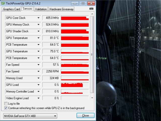
Sometimes you start into a review and it looks, on the surface, to be an easy one. Then later you realize that you just let yourself in for a few weeks of rigorous testing and easy left the room about the time you fired up the rig. This is one of those cases. What we boil down to a screenshot of GPU-Z ended up being 3 gaming sessions lasting hours, then pulling the median thermal reading.
Before we get into all that lets rehash a little GTX-480 info.
| GPU | GTX-480 | GTX-470 | GTX-285 | 5850 | 5870 | GTX-295 | 5970 |
|---|---|---|---|---|---|---|---|
| Shader units | 480 | 448 | 240 | 1440 | 1600 | 2x 240 | 2x 1600 |
| ROPs | 48 | 40 | 32 | 32 | 32 | 2x 28 | 2x 32 |
| GPU | GF100 | GF100 | GT200b | Cypress | Cypress | 2x GT200b | 2x Cypress |
| Transistors | 3200M | 3200M | 1400M | 2154M | 2154M | 2x 1400M | 2x 2154M |
| Memory Size | 1536 MB | 1280 MB | 1024 MB | 1024 MB | 1024 MB | 2x 896 MB | 2x 1024 MB |
| Memory Bus Width | 384 bit | 320 bit | 512 bit | 256 bit | 256 bit | 2x 448 bit | 2x 256 bit |
| Core Clock | 700 MHz | 607 MHz | 648 MHz | 725 MHz | 850 MHz | 576 MHz | 725 MHz |
| Memory Clock | 924 MHz | 837 MHz | 1242 MHz | 1000 MHz | 1200 MHz | 999 MHz | 1000 MHz |
| Price | $499 | $349 | $340 | $299 | $399 | $500 | $599 |
By now the specs of the GTX-480 are pretty well known. Pushing 3 billion transistors on a GPU die is an amazing feat in itself. Pushing 3 Billion transistors on one GPU die and controlling the heat is just as amazing as putting that many transistors on it in the first place.
Straight from Nvidia’s Mouth
This next section is Nvidia’s eloquent explanation on Fermi and it’s design. We could reword it and toss in a few comments and claim it as our own but frankly that would be a disservice to the fine folks over at Nvidia that came up with it. Let’s give credit where credit is due and if we have any comments to toss in this section, they will be in bold type.
NVIDIA’s Next Generation CUDA Compute and Graphics Architecture, Code-Named “Fermi”
The Fermi architecture is the most significant leap forward in GPU architecture since the original G80. G80 was our initial vision of what a unified graphics and computing parallel processor should look like. GT200 extended the performance and functionality of G80. With Fermi, we have taken all we have learned from the two prior processors and all the applications that were written for them, and employed a completely new approach to design to create the world’s first computational GPU. When we started laying the groundwork for Fermi, we gathered extensive user feedback on GPU computing since the introduction of G80 and GT200, and focused on the following key areas for improvement:
Improve Double Precision Performance—while single precision floating point performance was on the order of ten times the performance of desktop CPUs, some GPU computing applications desired more double precision performance as well.
- ECC support ECC allows GPU computing users to safely deploy large numbers of GPUs in datacenter installations, and also ensure data-sensitive applications like medical imaging and financial options pricing are protected from memory errors.
- True Cache Hierarchy some parallel algorithms were unable to use the GPU’s shared memory, and users requested a true cache architecture to aid them.
- More Shared Memory many CUDA programmers requested more than 16 KB of SM shared memory to speed up their applications.
- Faster Context Switching users requested faster context switches between application programs and faster graphics and compute interoperation.
- Faster Atomic Operations users requested faster read-modify-write atomic operations for their parallel algorithms.
With these requests in mind, the Fermi team designed a processor that greatly increases raw compute horsepower, and through architectural innovations, also offers dramatically increased programmability and compute efficiency. The key architectural highlights of Fermi are:
- Third Generation Streaming Multiprocessor (SM)
- 32 CUDA cores per SM, 4x over GT200
- 8x the peak double precision floating point performance over GT200
- Dual Warp Scheduler simultaneously schedules and dispatches instructions from tw
- independent warps
- 64 KB of RAM with a configurable partitioning of shared memory and L1 cache
- Second Generation Parallel Thread Execution ISA
- Unified Address Space with Full C++ Support
- Optimized for OpenCL and DirectCompute
- Full IEEE 754-2008 32-bit and 64-bit precision
- Full 32-bit integer path with 64-bit extensions
- Memory access instructions t
- support transition t
- 64-bit addressing
- Improved Performance through Predication
- Improved Memory Subsystem
- NVIDIA Parallel DataCacheTM hierarchy with Configurable L1 and Unified L2 Caches
- First GPU with ECC memory support
- Greatly improved atomic memory operation performance
- NVIDIA GigaThreadTM Engine
- 10x faster application context switching
- Concurrent kernel execution
- Out of Order thread block execution
- Dual overlapped memory transfer engines
An Overview of the Fermi Architecture
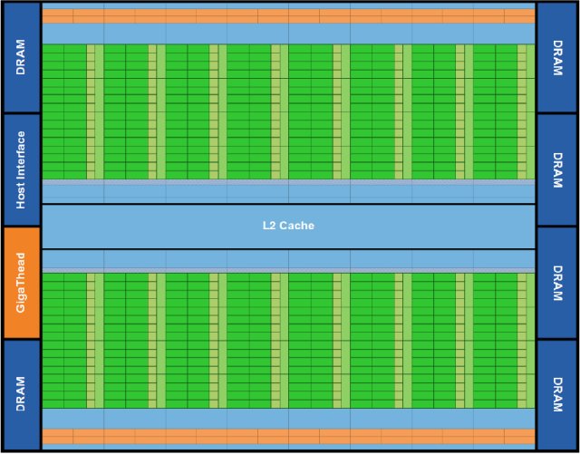
The first Fermi based GPU, implemented with 3.0 billion transistors, features up to 512 (GTX-480 has 480 cores exposed but has a total of 512 cores so we may see an enthusiast line with all 512 cores exposed at a later date, but notice the “up to 512 CUDA cores Nvidia let slip in the document) CUDA cores. A CUDA core executes a floating point or integer instruction per clock for a thread. The 512 CUDA cores are organized in 16 SMs of 32 cores each. The GPU has six 64-bit memory partitions, for a 384-bit memory interface, supporting up to a total of 6 GB of GDDR5 DRAM memory. A host interface connects the GPU to the CPU via PCI-Express. The GigaThread global scheduler distributes thread blocks to SM thread schedulers.
Third Generation Streaming Multiprocessor
The third generation SM introduces several architectural innovations that make it not only the most powerful SM yet built, but also the most programmable and efficient.
512 High Performance CUDA cores Each SM features 32 CUDA processors—a fourfold increase over prior SM designs. Each CUDA processor has a fully pipelined integer arithmetic logic unit (ALU) and floating point unit (FPU). Prior GPUs used IEEE 754-1985 floating point arithmetic. The Fermi architecture implements the new IEEE 754-2008 floating-point standard, providing the fused multiply-add (FMA) instruction for both single and double precision arithmetic. FMA improves over a multiply-add (MAD) instruction by doing the multiplication and addition with a single final rounding step, with no loss of precision in the addition. FMA is more accurate than performing the operations separately. GT200 implemented double precision FMA.
In GT200, the integer ALU was limited to 24-bit precision for multiply operations; as a result, multi-instruction emulation sequences were required for integer arithmetic. In Fermi, the newly designed integer ALU supports full 32-bit precision for all instructions, consistent with standard programming language requirements. The integer ALU is also optimized to efficiently support 64-bit and extended precision operations. Various instructions are supported, including Boolean, shift, move, compare, convert, bit-field extract, bit-reverse insert, and population count.
16 Load/Store Units
Each SM has 16 load/store units, allowing source and destination addresses to be calculated for sixteen threads per clock. Supporting units load and store the data at each address to cache or DRAM.
Four Special Function Units
Special Function Units (SFUs) execute transcendental instructions such as sin, cosine, reciprocal, and square root. Each SFU executes one instruction per thread, per clock; a warp executes over eight clocks. The SFU pipeline is decoupled from the dispatch unit, allowing the dispatch unit to issue to other execution units while the SFU is occupied.
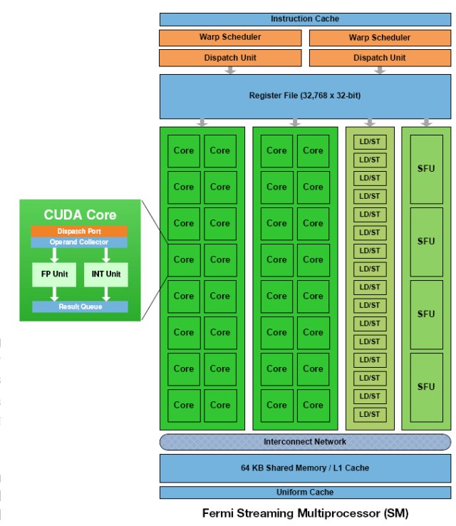
Fermi’s 16 SM are positioned around a common L2 cache. Each SM is a vertical rectangular strip that contain an orange portion (scheduler and dispatch), a green portion (execution units), and light blue portions (register file and L1 cache).
The Test Chassis
Normally we run tests on an open Top Deck Testing station but an open chassis design like that won’t work for this article. So we went with a Silverstone Raven 2 chassis that provides plenty of room. You can see the entire review of the Raven 2 HERE if you want to peruse it.
To make things a little easier lets insert a page from that review here to give you an idea of the chassis. No this isn’t a chassis article but the chassis is probably the single most important component in overall cooling in any system.


The Raven RV-02 is a little different from what we are used to. Removing the side panels on the Raven RV-02 required removal of the top porition of the chassis.


Then there are four thumb screws that secure the side panels onto the chassis. Remove the screws, swing the panels out a couple of inches, then lift straight up.

The design being solely based on an inverted 90° rotation of the motherboard, which means the PCI expansion cards go in through the rear and point upwards.

This chassis uses three 180mm fans on the bottom. With one 120mm fan up top. I see the 5.25″ drive bay is in the right spot, and this chassis uses a 3.5″ to 5.25″ HDD cage. Now I wonder where the PSU gets mounted at.

Looking at the PCI expansion openings on this chassis, a total of eight.

The included top mounted 120mm fan.

Better picture of one of the bottom 180mm fans. SilverStone uses a hex style grill to keep your fingers and small screws from entering.

This looks like where the PSU gets mounted at, it too is on a 90° angle.

As I suspected, the PSU gets mounted the same way the motherboard does. Right in front of the PSU mounting area are three little switches. These switches control the bottom three 180mm fans, a low and high speed setting. Now this baffled me, why use a fan controller on already quiet fans?

Moving towards the front of the chassis, you can make out the vented PCI expansion covers.

Each bottom 180mm fan has a removable filter. To remove the filters, all I had to do was grab the tab, lift up, and slide it right out.

The fresh air intake for the PSU.

The 3.5″ to 5.25″ HDD cage, this HDD cage can only house three 3.5″ HDD’s.

Since our components are mounted pointing upwards, SilverStone made this chassis step down a bit so we can hide all of our cables.

Here is the Raven RV-02 chassis top cover. This is vented so the computer components can breath. Since heat rises, the design of this chassis makes sense.

A quick snapshot of the SilverStone logo on the Raven RV-02 chassis.

The PSU intake has a removable filter on it as well.

Looking at the rear external portion of the chassis.

Here we put the Raven RV-02 chassis on its side to look at the bottom. The entire bottom is well ventilated to allow airflow to the bottom mounted 180mm fans. If you look closely at the bottom of the chassis you can make out two small holes.

This is for those with an external water cooling set up. What i thought was a bit odd was that these are located here. Running our hoses from the bottom of the chassis is begging for kinks when trying to make that sharp radius.

The front bottom of the chassis.


Time to turn our attention to the 180mm fans once again. We can remove the bottom 180mm fans to either clean them, replace them, or if we wanted, install a water cooling radiator. Remove the two screws that are in front of the fans, then slide them out. Similar to removing the filter.
NOTE: You also have to remove the top three fan control switches to fully remove the bottom 180mm fans.


Here is what the fans look like that were used in this chassis.


The 5.25″ drive bays are a screw-less design.

SilverStone includes 2 front I/O USB ports with front audio headers, these are located up top in the front.

On the outer edges of the top portion are the ON/OFF and reset buttons.


The HDD cage is held in by eight thumbscrews, there are 4 on each side.

The HDD cage has rubber isolation mounts mounted directly to the cage to reduce vibrations from the HDDs.
The Test Rig
Since we had a look at the chassis we need to look at what we have installed in the test rig. We didn’t take it easy on the article, we packed the chassis with everything but the kitchen sink. This is a full fledged enthusiast system with a Core i7 980x, 3x SAS Hard drives, 2x SSD’s, hardware Raid card, and about as much extremely expensive hardware as we could cram into it as we could get.
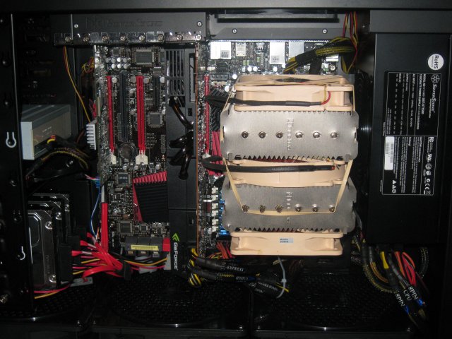
We didn’t go skimpy in this chassis. At the end of the day we have to live with the build on a day to day basis and you don’t strip out a chassis just to keep things tidy. We did make every effort to wire the chassis tightly and keep wires out of the way as much as possible. We do that anyway, a bunch of wires hanging around looking ugly can ruin the look of a rig as well as the airflow.
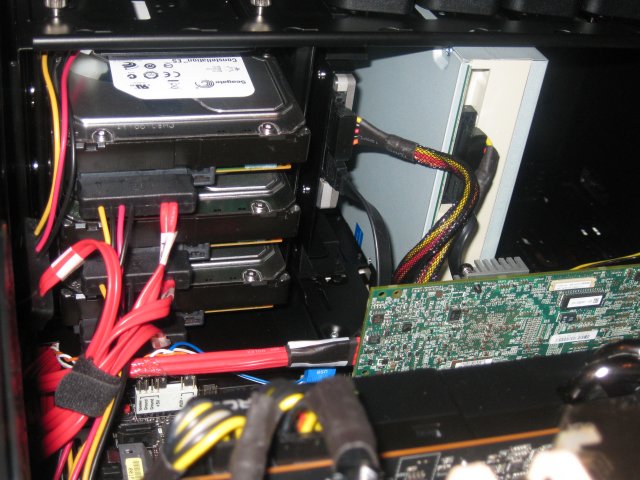
Over toward the drive bays you can see the three Seagate Constellation SAS 6Gb/s hard drives, one of the two SSD’s and the Asus Blu-Ray combo drive. You also get a peek at the 3Ware hardware RAID controller.
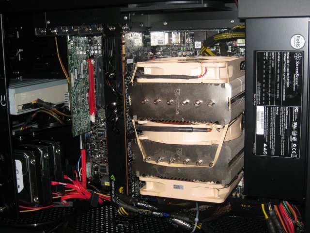
That’s a full sized Silverstone Strider 1500W PSU and we used the Noctua NH-D14 dual tower CPU cooler and used 3 120mm Noctua fans. In other words we didn’t strip out the chassis, we loaded it heavier than most chassis can ever dream of being loaded. How heavy, figure the Drives, CPU, GPU, Raid Card run close to $4k, not to mention the 1500w PSU, the Raven 2, the Rampage 3, the CPU cooler, or the 12 GB of ram. It’s a dream machine and the chassis is packed with goodies so the first e-mailer that says “Oh they stripped the chassis” we will send some secret Bjorn3D Ninja’s and they will steal away into the night with your gaming shrine.
Test Rig Specifics
| Test Rig “Quadzilla” |
|
| Case Type | Silverstone Raven 2 |
| CPU | Intel Core I7 980 Extreme |
| Motherboard | Asus Rampage 3 |
| Ram | Kingston HyperX 12GB 9-9-9-24 |
| CPU Cooler | Noctua NH-D14 (3x 120mm fans) |
| Hard Drives |
3x Seagate Constellation ES 2TB 7200 RPM 16MB Cache |
| Optical | Asus BD-Combo |
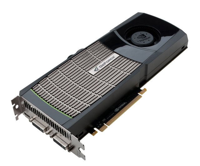
| GPU | Nvidia GTX-480 |
| Case Fans | 120mm Fan cooling the mosfet CPU area |
| Docking Stations | None |
| Testing PSU | Silverstone Strider 1500 Watt |
| Legacy | None |
| Mouse | Razer Lachesis |
| Keyboard | Razer Lycosa |
| Gaming Ear Buds |
Razer Moray |
| Speakers | None |
| Any Attempt Copy This System Configuration May Lead to Bankruptcy | |
Please note that all tests were performed with the chassis sides on and absolutely no extra cooling. Just the Raven 2 with it’s built in cooling. The only other fans in the chassis were on the power supply, the GPU, and the CPU cooler. No extra fans were stuffed in there, no fans were sitting outside the chassis providing extra airflow. Just the Raven 2 with it’s low RPM fans.
Methodology and Software Used
Initially we were going to just run games. Then the article got more grandiose in scale and we included Furmark, ATITool, 3DMark Vantage, several stand alone game benchmarks and of course games.
We ran Furmark for 5 minutes, for an explanation on that see the next page. We also ran Furmark for 30 minutes on a lot of the modern GPU’s and built a table for it. ATITool we ran for 10 minutes, stand alone benchmarks we ran 5 passes at the benchmark then recorded the temperature. In Crysis we ran 10 complete passes of the Frame buffer Benchmark tool. In Games we ran the games on the absolute highest setting you can use. Each game we gamed for 2 hours then recorded the temperatures. We did 3 gaming sessions for each game totaling 6 hours. Each session was back to back with nothing but a pause for taking a screenshot of GPU-Z. We didn’t let the GPU cool down at all between sessions. We report the highest temperature we got during sessions.
Of course we used a fresh load of Windows 7 64 bit Ultimate and updated it and all the drivers to the latest versions. All the games were patched to the latest patch, all the benchmarks were the latest releases.
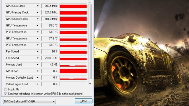
Keep in mind we aren’t looking at performance, we are looking at the temperatures the GTX-480 generates so we went with screenshots because we want you to see the GPU-Z screen superimposed on the game or benchmark we were running so there is no doubt what temperature the GPU was running at.
We went to great pain to ensure the ambient temperature was at 72°F and no breezes or fans were blowing on the chassis at any time. The chassis itself was on a wooden surface clear of dust and debris. We didn’t disable anything in Windows, or tweak the rig or GPU in any way. We ran at stock CPU speed, stock Ram speed and stock GPU speed.
Lastly before we get to the software used we’d like to say we get inundated with E-Mail on a daily basis, E-Mails ranting about the temperatures will be deleted en-mass. These are screenshots of the GTX-480 in the Raven 2 and as such leave little doubt as to the resulting temperature. If you have specific concerns address them politely and if we get time we will respond.
Synthetic Benchmarks & Games
| Synthetic Benchmarks & Games | |
| 3DMark Vantage | |
| World In Conflict Benchmark | |
| Metro 2033 | |
| Call of Duty Modern Warfare 4 | |
| FarCry 2 | |
| Stalker COP | |
| Crysis Warhead | |
| Unigine Heaven v.2.0 | |
| Intel DX11 SDK | |
| ATITool | |
| Furmark | |
| Batman Arkham Asylum | |
| Battlefield Bad Company 2 | |
| Dirt 2 | |
| Dual Monitor | |
| Left 4 Dead 1 | |
| Nvidia Rocket Sled Demo | |
| Stone Giant | |
We ran 18 total games and benchmarks to get a good representative sample of what you can expect, thermally speaking, from the GTX-480.
Furmark
Methodology and Software Used
Initially we were going to just run games. Then the article got more grandiose in scale and we included Furmark, ATITool, 3DMark Vantage, several stand alone game benchmarks, and of course games.
Furmark we ran for 5 minutes. Why 5 minutes? Furmark is unrealistic in thermal measurement of GPU’s and bypasses normal GPU hardware and drives up temperatures. It’s designed like Intel Burn for CPU’s it heats them up as hot as they will go. You will never see a game or application that heats up your GPU like Furmark does. We don’t like the program as it misleads a lot of people about the real temperatures you can expect from your GPU. As long as we are here we went ahead and ran Furmark on several GPU’s and this is the only time we will looking at multiple GPU’s in this article. Until later anyway when we toss this table back up.
| Geforce GTX-480 | 96 |
|---|---|
| Geforce GTX-470 | 95 |
| Radeon HD 5970 | 95 |
| Radeon HD 5870 | 92 |
| Geforce GTX-295 | 92 |
| Geforce GTX-285 | 91 |
| Radeon HD 4870×2 | 86 |
| Radeon HD 5850 | 81 |
Every GPU listed here is a stock reference speed GPU, none are overclocked, every one was tested in the same exact rig, same ambient temperature, same version of Furmark, same 30 minute run. So for what it is worth we could actually stop here and say stop whining about the GTX-480 temperatures. The HD 5970 was 1°C lower than the GTX-480 and the same temperature as the GTX-470. The HD 5870 was 4°C lower than the GTX-480. The GTX-285 was 5°C lower than the GTX-480. The HD 5870 will throttle at 100°C so it has 8°C left, the GTX-480 throttles at 105°C so it has 9°C left yet the screaming about the thermals on the GTX-480 were ripped apart. I don’t remember anyone screaming about the 5870 or the 5970 yet they have less overhead to throttle than the GTX-480 and have far less transistors to service per core. Each core on the HD 5870 and HD5970 have 2.154 Billion Transistors and come within 4°C of the GTX-480 which supports 0.846 Billion or 846 Million more transistors.
It’s a given that the die on the HD 5870 is smaller than Fermi’s die size so in all fairness the HD 5870 is dissipating it’s heat across a smaller die but what does that mean to the end user as far as heat goes. Nothing at all, what we care about is how hot it got not how hot it get’s per square millimeter. (GTX-480 528mm², HD 5870
334mm² die size).
All that being said it’s still by Furmark which presents unrealistic temperatures but since most of the review sites were reporting GTX-480 temperatures with Furmark we though we’d set the record straight. If you want to scream about temperatures do so in a fair manner. All the modern GPU’s run hot in Furmark, Furmark is designed to run them hot and isn’t representative of real life temperatures.
Here’s a screenshot of Furmark on the GTX-480 after 5 minutes.
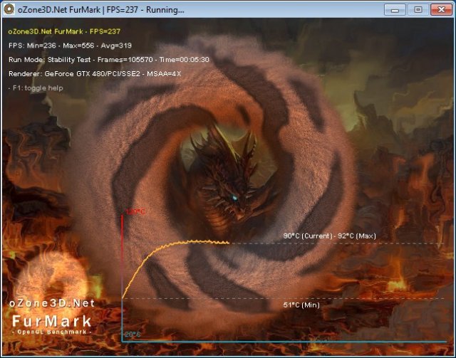
We topped out at 92°C after a 5 minute run so the additional 25 minutes we ran for the table and the GTX-480 gained 4°C and no matter how long we ran the test the GTX-480 refused to throttle.
ATITool
ATITool has been around for a long long time, all we use it for is checking for artifacts and heating up GPU’s. Even with it’s age it still manages to run GPU’s at 90 – 100% core usage and is a little unrealistic in that. Games will vary GPU usage from minute to minute and that gives the GPU a chance to cool down a little, non-game utilities like ATITool don’t do that they hammer the GPU non-stop.
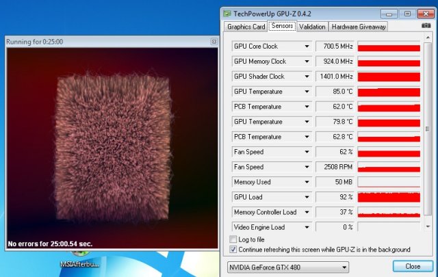
So in ATITool we got a temperature of 85°C and in this run we went 25 minutes which is 15 minutes longer than we normally run. Even out there at 25 minutes we didn’t see any increase in temperatures after 10 minutes and the noise from inside the chassis at 62% fan was almost inaudible. We ran all the tests on auto fan which is another good reason for the screenshots. You can see the fan speed and know we weren’t hopping the fan to 100%.
Batman Arkham Asylum
Batman: Arkham Asylum is an action-adventure stealth video game based on DC Comics’ Batman for the PlayStation 3, Xbox 360 and Microsoft Windows. It was developed by Rocksteady Studios and published by Eidos Interactive in conjunction with Warner Bros. Interactive Entertainment and DC Comics. The PS3 and Xbox 360 versions of the game were released on August 25, 2009 in North America and August 28, 2009 in Europe, and the PC version was released on September 15 in North America and on September 18 in Europe.
Arkham Asylum, written by veteran Batman writer Paul Dini, is based on the long-running comic book mythos, as opposed to most other Batman games which are adaptations of the character in other media besides the source material. The Joker, Batman’s arch enemy, has instigated an elaborate plot from within Arkham Asylum where many of Batman’s other villains have been incarcerated. Batman investigates and comes to learn that the Joker is trying to create an army of Bane-like creatures that threaten Gotham City, and is forced to put a stop to the Joker’s plans. The game’s main characters are voiced by the actors from the DC Animated Universe, namely Kevin Conroy, Mark Hamill, and Arleen Sorkin reprise their roles as Batman, the Joker, and Harley Quinn, respectively. The game is played as a third-person perspective action-adventure game with a primary focus on Batman’s combat abilities, his stealth and detective skills, and an arsenal of gadgets that can be used in both combat and exploration.
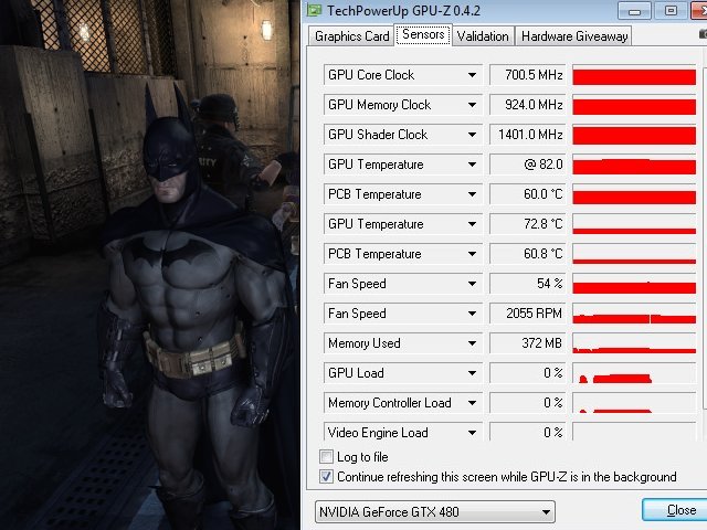
Some of the screenshots we weren’t quite fast enough on and the GPU temperature dropped a hair. We put the cursor over the hottest point on the GPU-Z bar and that results in the “@ 82.0” instead of “82.0”. What you are seeing is the highest temperature we got on exit from Batman and that was 82°C after a total of 6 hours gaming. That leaves us 23°C to the maximum operating temperature of 105°C.
Battlefield Bad Company 2
Battlefield Bad Company™ 2 brings the spectacular Battlefield gameplay to the forefront of next-gen consoles and PC, featuring best-in-class vehicular combat set across a wide range of huge sandbox maps each with a different tactical focus. New vehicles like the All Terrain Vehicle (ATV) and the UH-60 transport helicopter allow for all-new multiplayer tactics in the warzone. Extensive fine-tuning ensures that this will be the most realistic vehicle combat experience to date. Tactical destruction is taken to new heights with the updated DICE Frostbite engine. Players can now take down entire buildings or create their own vantage points by blasting holes through cover, thereby delivering a unique dynamic experience in every match.
Players can also compete in 4-player teams in 2 exclusive squad-only game modes, fighting together to unlock exclusive team awards and achievements. Spawn on your squad to get straight into the action and use gadgets such as the tracer dart in conjunction with the RPG to devastating effect. Excellence in the battlefield is rewarded with an extensive range of pins, insignias and stars to unlock along with 50 dedicated ranks to achieve. Variety also extends into the range of customizable kits weapons and vehicles available. With 4 distinct character classes, dozens of weapons, several gadgets and specializations, players have over 15,000 kit variations to discover and master. Players will be able to fine-tune their preferred fighting style to give them the edge in combat.
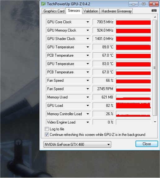
Battlefield Bad Company 2 got the GTX-480 up to 89°C after 6 hours of gaming at the highest settings. Between each 6 hour gaming session we turned the rig off and let it cool down. We did have to tag team the 6 hour sessions and switch out gamers. We had no shortage of qualified gamers wanting a shot at Hexzilla which is normally strictly off limits to anyone else. This is the first and only time anyone will ever have access to Hexzilla.
Dual Monitor Testing
Dual monitor testing is pretty self explanatory. We fired up two monitors and tested the idle temperature. We also fired up Heaven 2 and benched it 5 times and took a screenshot of the temperature of the final run.
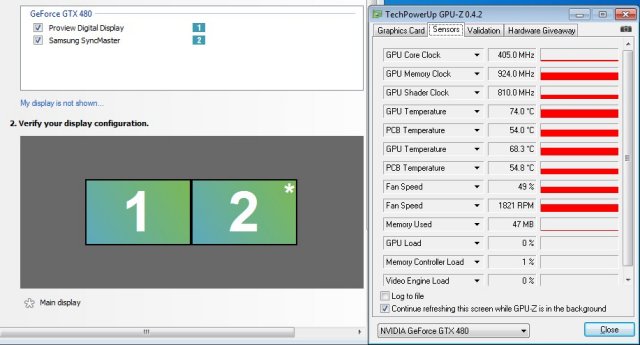
To keep the screen from flickering on dual monitor Nvidia had to keep the memory speed high so Dual monitor idle runs hotter than single monitor idle. Which is why we wanted to test it. We got 74°C at an idle after 30 minutes.
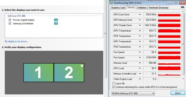
After 5 complete runs of the Heaven 2 benchmark we got 89°C and it looks like temperatures might have hit 90°C so we still have 15°C to the throttle temperature after about an hour of benching.
Call of Duty 4 Modern Warfare
Call of Duty 4: Modern Warfare is a first-person shooter video game, developed by Infinity Ward and published by Activision for the Xbox 360, PlayStation 3 and Wii video game consoles and the Microsoft Windows and Mac OS X operating systems. The game was released in North America, Australia, and Europe in November 2007 for video game consoles and Windows, was released for the Mac in September 2008, and was released for the Wii (named ‘Reflex Edition’) in November 2009.[1] It is the fourth installment in the Call of Duty video game series, excluding expansion packs, and is followed by a direct sequel, Call of Duty: Modern Warfare 2. The game breaks away from the World War II setting of previous games in the series and is instead set in modern times. Call of Duty 4 was in development for two years, and it uses a proprietary game engine.
The story takes place in a fictional near-future, where a radical leader has staged an execution order against the president of an unnamed country in the Middle East, and an “Ultranationalist” movement has instigated a civil war in Russia. The events of the conflicts are seen from the perspectives of a U.S. Reconnaissance Marine and a British SAS commando, and are set in multiple locations, including the Middle East, Azerbaijan, Russia, and Prypiat, Ukraine. The multiplayer portion of the game features various game modes, and contains a leveling system that allows the player to unlock additional weapons, weapon attachments, and camouflage schemes as they advance.
We ended up getting 83°C and the 81°C you see here is the short lag between hitting Alt-Tab to get back to the desktop and hitting the button for our screen capture program. At 83°C we still have 22°C to the 105°C throttle point after 6 hours gaming.
Dirt 2
Colin McRae: Dirt 2 (known as Dirt 2 outside Europe and stylised, DiRT)is a racing game released in September 2009, and is the sequel to Colin McRae: Dirt. This is the first game in the McRae series since McRae’s death in 2007. It was announced on 19 November 2008 and features Ken Block, Travis Pastrana, Tanner Foust, and Dave Mirra. The game includes many new race-events, including stadium events. Along with the player, an RV travels from one event to another, and serves as ‘headquarters’ for the player. It features a roster of contemporary off-road events, taking players to diverse and challenging real-world environments. The game takes place across four continents: Asia, Europe, Africa and North America. The game includes five different event types: Rally, Rallycross, ‘Trailblazer,’ ‘Land Rush’ and ‘Raid.’ The World Tour mode sees players competing in multi-car and solo races at new locations, and also includes a new multiplayer mode.
Colin McRae: Dirt is the first PC video game to use Blue Ripple Sound’s Rapture3D sound engine by default.
A demo of the game was released on the PlayStation Store and Xbox Live Marketplace on 20 August 2009. The demo appeared for the PC on 29 November 2009; it features the same content as the console demo with the addition of higher graphic settings and a benchmark tool
In Dirt 2 we had to have some younger help to game for 6 hours. Being in the over 50 crowd racing games aren’t our forte so we enlisted the help of a 13 year old dedicated gamer and turned him loose with a six pack of Mountain Dew and a variety of sugary treats.
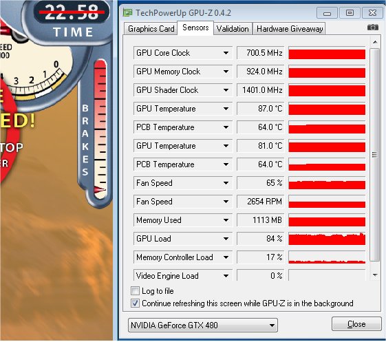
In the six hour gaming session we came out with a reading of 83°C and we expect a 2°C drop for the lag time between game and screenshot so 85°C and still after 6 hours intensive gaming with a hopped up 13 year old on Mountain Dew and about a half pound of sugar we still have 20°C to the throttle point.
On a side note the 13 year old did survive but his Mother wasn’t very happy with us for several days after. Hey six hours gaming on Hexzilla requires a good caloric intake but we do apologize to the mother for the hole in her screen door. After gaming he walked right through the screen door without opening it. Our bad Ma. (It wasn’t the sugar it was the excitement of seeing a game played correctly on a top end GPU and we suspect he was headed for a hammer and his game console)
Far Cry 2
Far Cry 2 (commonly abbreviated as “FC2”) is an open-ended first-person shooter developed by Ubisoft Montreal and published by Ubisoft. It was released on October 21, 2008 in North America and on October 23, 2008 in Europe[3] and Australia. It was made available on Steam on October 22, 2008.[9] Crytek, the developers of the original game, were not involved in the development of Far Cry 2.
Ubisoft has marketed Far Cry 2 as the true sequel to Far Cry, though the sequel has very few noticeable similarities to the original game. Instead, it features completely new characters and setting, as well as a new style of game play that allows the player greater freedom to explore different African landscapes such as deserts, jungles, and savannas. The game takes place in a modern-day East African nation in a state of anarchy and civil war. The player takes control of a mercenary on a lengthy journey to locate and assassinate “The Jackal,” a notorious arms dealer.
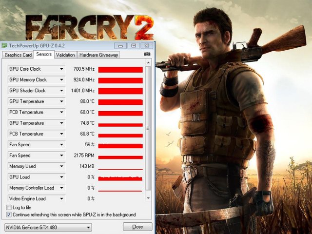
Far Cry 2 sees the GTX-480 hitting 80°C after a grueling 6 hour run at it. Like we mentioned we stopped at 2 hours, 4 hours and 6 hours just long enough to get screenshots then right back to the game. Six hours is a long gaming session for us but we wanted to make sure that the temperatures were taken in real life settings after exhaustive gaming. You don’t buy a GTX-480 to play Solitaire for 10 minutes. The GTX-480 is a gaming weapon.
Unigine Heaven 2.0
Heaven Benchmark is a DirectX 11 GPU benchmark based on advanced Unigine™ engine from Unigine Corp. It reveals the enchanting magic of floating islands with a tiny village hidden in the cloudy skies. Interactive mode provides emerging experience of exploring the intricate world of steampunk.
- Support of DirectX 9, DirectX 10, DirectX 11 and OpenGL 4.0
- Comprehensive use of tessellation technology
- Advanced SSAO (screen-space ambient occlusion)
- Volumetric cumulonimbus clouds generated by a physically accurate algorithm
- Simulation of changing light conditions
- Dynamic sky with light scattering
- Interactive experience with fly/walk-through modes
- Stereo 3D modes:
- Anaglyph
- Separate images
- 3D Vision
- iZ3D
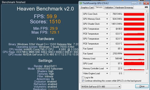
Heaven 2 has so many advanced features that it heats up the GTX-480 really well. What we found was that games with Tessellation and/or Ray tracing did a nice job of heating it up. Heaven was no exception and we got 88°C after 5 back to back runs. Heaven isn’t a short benchmark so the GPU was running about an hour almost non-stop. Here at 65% fan speed inside the chassis the GPU was barely audible.
Left 4 Dead
Left 4 Dead is a cooperative first-person shooter video game. It was developed by Turtle Rock Studios, which was purchased by Valve Corporation during development. The game uses Valve’s proprietary Source engine, and is available for Windows and the Xbox 360. Development on the game was completed on November 13, 2008 and was released digitally on November 17, 2008 and at retail on November 18, 2008 in North America, In Australia on November 18, 2008 and on November 21, 2008 in Europe and Japan.
Set during the aftermath of an apocalyptic pandemic, the game pits its four protagonists—dubbed the “Survivors”—against hordes of the infected. There are four game modes: a single-player mode in which allied characters are controlled by AI; a four-player, co-op campaign mode; an eight-player online versus mode; and a four-player survival mode. In all modes, an artificial intelligence (AI), dubbed the “Director”, controls level pacing and item spawns, in an attempt to create a dynamic experience and increase replay value.
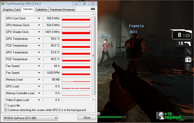
Left 4 Dead saw the GTX-480 at 59°C and you can tell this epic title isn’t any sort of challenge for the GTX-480. Still though there’s nothing like wading through waist deep Zombies with a 10 round automatic shotgun at your disposal.
Metro 2033
Metro 2033 is an action-oriented video game with a combination of survival horror, and first-person shooter elements. The game is based on the novel Metro 2033 by Russian author Dmitry Glukhovsky. It was developed by 4A Games in Ukraine and released in March 2010 for the Xbox 360 and Microsoft Windows. In March 2009, 4A Games announced a partnership with Glukhovsky to collaborate on the game. The game was announced a few months later at the 2009 Games Convention in Leipzig; a first trailer came along with the announcement. When the game was announced, it had the subtitle The Last Refuge but this subtitle is no longer being used by THQ.
The game is played from the perspective of a character named Artyom. The story takes place in post-apocalyptic Moscow, mostly inside the metro system where the player’s character was raised (he was born before the war, in an unharmed city), but occasionally the player has to go above ground on certain missions and scavenge for valuables.
The game’s locations reflect the dark atmosphere of real metro tunnels, albeit in a more sinister and bizarre fashion. Strange phenomena and noises are frequent, and mostly the player has to rely only on their flashlight to find their way around in otherwise total darkness. Even more lethal is the surface, as it is severely irradiated and a gas mask must be worn at all times due to the toxic air. Water can often be contaminated as well, and short contacts can damage the player, or even kill outright.
Often, locations have an intricate layout, and the game lacks any form of map, leaving the player to try and find its objectives only through a compass – weapons cannot be used while visualizing it. The game also lacks a health meter, relying on audible heart rate and blood spatters on the screen to show the player what state they are in and how much damage was done. There is no on-screen indicator to tell how long the player has until the gas mask’s filters begin to fail, save for a wristwatch that is divided into three zones, signaling how much the filter can endure, so players must continue to check it every time they wish to know how long they have until their oxygen runs out, requiring the player to replace the filter (found throughout the game). The gas mask also indicates damage in the form of visible cracks, warning the player a new mask is needed. The game does feature traditional HUD elements, however, such as an ammunition indicator and a list of how many gas mask filters and adrenaline shots (med kits) remain.
Another important factor is ammunition management. As money lost its value in the game’s setting, cartridges are used as currency. There are two kinds of bullets that can be found, those of poor quality made by the metro-dwellers themselves, which are fairly common but less effective against targets, especially mutants, and those made before the nuclear war, which are rare and highly powerful, but are also necessary to purchase gear or items such as filters for the gas mask and med kits. Thus, the player is forced to manage their resources with care.
Metro 2033 is probably the most advanced game of 2010 and the bells and whistles it offers can bog down almost any GPU we’ve seen. So in this case we were playing at out of the box settings because playing 6 hours with lag and stutter would be brain numbing. That’s no reflection on the GTX-480 they designed the game along the Crysis mentality. “Lets make a game so hard to run no existing GPU will run it well” (and maybe it’ll be as famous as Crysis and sell well).
In Metro 2033 (which I actually play and like) we got 83°C after endless hours of gaming. I did stop at 2 and 4 hours and grab a screen shot but time slipped by and I was well past the 6 hour point when we noticed dawn making it’s first little crack. At which point I quickly screenshot GPU-Z shut the rig down and made breakfast and took it to my better half who thought I got up early and made breakfast for her. (Bonus game all night and get brownie points)
Nvidia Sled Demo
The Nvidia Sled Demo ships with the GTX-4xx lineup of GPU’s and since we aren’t comparing the GTX-480 we felt free to fire it up and take readings. Besides it’s kinda fun to watch that little dude flying through the air. We did 5 passes at the benchmark then took the thermal reading.
The Sled demo is kind of short but we were just throwing it in for fun anyway, after gaming for 2 weeks with intensive 6 hour sessions we needed a little comic relief. The GTX-480 hit 87°C in the Sled Demo and even extending out to 10 runs didn’t increase the temperature.
We apoligize a screenshot of the Rocket Sled Demo with a manually set fan was initially posted. That has been corrected and this screenshot is with the fan set to auto.
Stalker COP
S.T.A.L.K.E.R.: Call of Pripyat is the sequel to S.T.A.L.K.E.R.: Shadow of Chernobyl, a first-person shooter computer game by Ukrainian developer GSC Game World. S.T.A.L.K.E.R.: Call of Pripyat is the third game in the survival FPS S.T.A.L.K.E.R. series.
The events of S.T.A.L.K.E.R.: Call of Pripyat unfold shortly after the end of S.T.A.L.K.E.R.: Shadow of Chernobyl following the ending in which Strelok destroys the C-Consciousness. Having discovered the open path to the Zone’s center, the government decides to stage a large-scale operation to take control of the Chernobyl nuclear plant.
According to the operation’s plan, the first military group is to conduct an air scouting of the territory to map the anomalous fields. Thereafter, making use of the maps, the main military forces are to be dispatched.
Despite thorough preparations, the operation fails. Most of the advanced helicopters crash. In order to collect information on the reasons for the operation’s failure, Ukraine’s Security Service send their agent (protagonist – Alexander Degtyarev) into the Zone. From now on everything depends on the player.
The player must traverse through the Zone and investigate the crash sites. As the player progresses he starts learning why the helicopters crashed. The climax of the story begins when the player reaches Pripyat to find survivors of the helicopter crashes. The player eventually meets Strelok from the original S.T.A.L.K.E.R. game (Shadow of Chernobyl) and learns of the secrets behind the Zone.
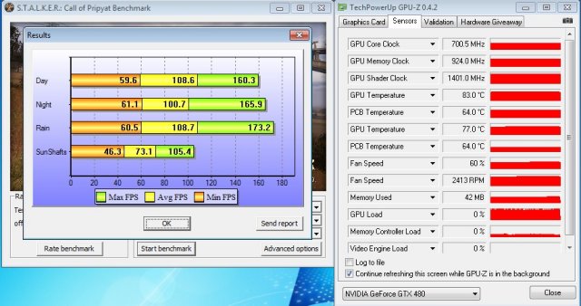
By this time we were close to delirious and got 5 runs at 1280×1024 before we realized we weren’t at 1920×1200 so we thought it would be interesting to see if resolution affected temperatures. At 1280×1024 we saw 83°C.
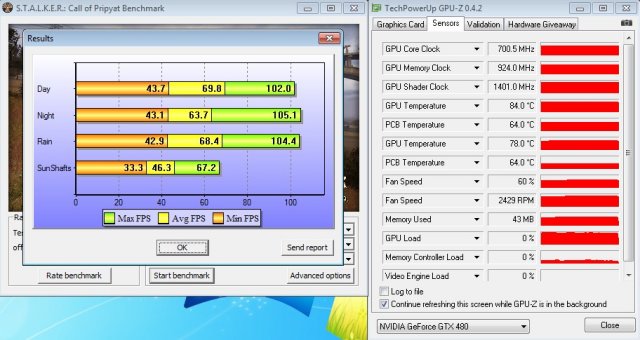
Moving to 1920×1200 we got 84°C and from 1280×1024 to 1920×1200 we got a mere 1°C temperature increase and that’s not enough to say resolution is seriously affecting the thermal properties of the GTX-480.
Stone Giant
Game engine developer BitSquid, and game developer Fatshark, both based in Stockholm, Sweden, today jointly announced “StoneGiant”, a demo designed to showcase the power of Microsoft DirectX 11 technology.
StoneGiant allows consumers to test the overall performance of their consumer-based GPUs. Based on the BitSquid Tech, StoneGiant has primarily been used to test the tools and technology in a real-world production environment with the talented artists of Fatshark. Starting today, press can request to download the beta version of StoneGiant (contact [email protected]), with the public Stone Giant demo expected to be released in two weeks.
“With DX11 hardware becoming more readily available, we decided now would be a good time to highlight the advanced features of our engine, including DX11 and tessellation support,” said Tobias Persson, Lead Engineer at BitSquid. “Tessellation adds an awful lot to the visual fidelity of the scene and is something that consumers can readily see for themselves. We are looking forward to seeing how games will take advantage of our engine.”
BitSquid Tech is available for licensing soon for the PC, with PS3 and Xbox360 versions available by Q3 of 2010.
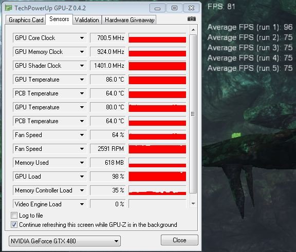
Stone Giant sees the GTX-480 hitting 86°C after 5 runs. If you are a regular reader you will have noticed the first run was 96 FPS. We were playing with the control on the Tech Demo on the first run so we got a different outcome. The following 4 runs were all at 75 FPS and that’s as consistent as we’ve seen any benchmark. The tech demo makes heavy use of Tessellation and heated up the GPU pretty good. Even at 86°C we still have 19°C left until the GPU throttles. We went ahead and extended testing to 15 runs but it didn’t make the GPU any hotter. Once the GTX-480 hits stride the temperature doesn’t creep up like a lot of GPU’s, it hit’s it’s temperature and stays there within 1 – 2°C.
3DMark Vantage
For complete information on 3DMark Vantage Please follow this Link:
www.futuremark.com/benchmarks/3dmarkvantage/features/
The newest video benchmark from the gang at Futuremark. This utility is still a synthetic benchmark, but one that more closely reflects real world gaming performance. While it is not a perfect replacement for actual game benchmarks, it has its uses. We tested the thermal properties of the GTX-480 with every setting set as high as it will go.
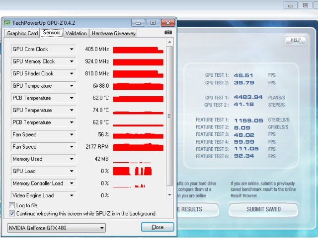
Vantage we almost didn’t run and were a little amazed the GTX-480 hit 88°C in the benchmark. One thing it did show us is that the fan profile on the GTX-480 is adjusting on the fly and here again we didn’t notice any annoying fan noise inside the chassis. Most of the noise reports we saw were open chassis tests with the fan at 100% and in extensive testing we’ve never seen the fan (on auto) get above 70% and at that level inside a chassis it’s not noisy.
Crysis Warhead
Crysis Warhead, like the original, Crysis, is based in a future where an ancient alien spacecraft has been discovered beneath the Earth on an island east of the Philippines. The single-player campaign has the player assume the role of (Former SAS) Delta Force operator Sergeant Michael Sykes, referred to in-game by his call sign, Psycho. Psycho’s arsenal of futuristic weapons builds on those showcased in Crysis, with the introduction of Mini-SMGs which can be dual-wielded, a six-shot grenade launcher equipped with EMP grenades, and the destructive, short ranged Plasma Accumulator Cannon (PAX). The highly versatile Nanosuit returns. In Crysis Warhead, the player fights North Korean and extraterrestrial enemies, in many different locations, such as a tropical island jungle, inside an “Ice Sphere”, an underground mining complex, which is followed by a convoy train transporting an unknown alien object held by the North Koreans, and finally, to an airfield. Like Crysis, Warhead uses Microsoft’s new API, Direct3D 10 (DirectX 10) for graphics rendering. Crytek have also recently added a Crysis Wars mod for the Sandbox 2 editor, the same tool that Crytek used to create the game.

We did 10 full passes at the Frame Buffer Warhead benchmark and got 90°C So we were looking at 90°C and even though Crysis is getting old it still stresses GPU’s because the GTX-480 FPS average was 32.2 FPS. Seems strange that we get 32.2 FPS but it heats the GPU to 90°C but Crysis lacks heavy Tessellation and ray tracing so it’s not stressing all of the GTX-480. Here’s the crux of the matter though, GTX-480 packs 3 Billion transistors onto a single Die, it’s going to get hot. Think of it this way GTX-295 with it’s dual core design packs 2.8 Billion got just as hot and noone thought twice about that. Stuff more transistors onto a single die, add new features, teach it to eat tessellation for lunch and suddenly heat becomes a problem.
World In Conflict
World in Conflict, or WiC, is a real-time tactical video game developed by the Swedish video game company Massive Entertainment and published by Ubisoft (formerly Sierra Entertainment) for Microsoft Windows. The game was released in September 2007. An expansion pack was released in March 2009 under the name World in Conflict: Soviet Assault; however, the console version has since been dropped from its productions by Activision and instead only exists as the expansion to the PC version.
The game is set in 1989 during the social, political, and economic collapse of the Soviet Union. However, the title postulates an alternate history scenario where the Soviet Union pursued a course of war to remain in power.
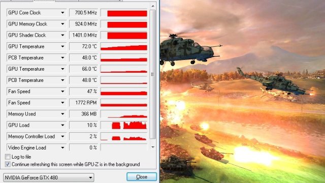
With World in Conflict we used the Demo and we made one pass at the demo. Face it, by now we were ready to die of bench exhaustion. That and the time it takes to restart the demo was letting the GPU cool down some so we settled for a single run. From an idle single run we got 72°C. The game is old enough we probably don’t need to go any farther with it anyway.
Conclusion
That’s pretty much it for our thermal study on the GTX-480. We saw temperatures range from around 59°C to upwards of 90°C in the most grueling conditions we could think of. The GTX-480 isn’t the coolest running GPU we’ve ever seen but initial reports of 96°C stemming from Furmark got it a lot of attention. If we had to place an average temperature on the GTX-480 we would say between 75 – 85°C with about 20°C of overhead left until it would throttle.
We also ran thermal tests on an open Top Deck Testing station and a HAF-932 chassis and the TOP Deck testing station came in with cooler temperatures. Since it’s an open design we didn’t present those numbers. The HAF-932 produced simular results to the Raven 2 and we will present a sample of those results in a shorter thermal study at a later date. Face it the six hour gaming runs we used in this study put us a little behind so we have to get a few other products finished before we go any farther.
The GTX-480 runs hot but it runs fast and handles this generation gaming effects well. With DX11 and Tessellation making such a large splash in the gaming industry it’s fairly amazing Nvidia got ahead of the technology curve at all.
When you think of the initial reports of the heat generated from the GTX-480 remember this table.
| Geforce GTX-480 | 96 |
|---|---|
| Geforce GTX-470 | 95 |
| Radeon HD 5970 | 95 |
| Radeon HD 5870 | 92 |
| Geforce GTX-295 | 92 |
| Geforce GTX-285 | 91 |
| Radeon HD 4870×2 | 86 |
| Radeon HD 5850 | 81 |
There’s the cut and dried of it. Early reports were done in Furmark with no thought of actual real life performance and in Furmark the difference between the GTX-480 and the HD 5870 was a mere 4°C.
When the GTX-295 came out it was heralded as a breakthrough dual core GPU and it didn’t receive any of the harping that the GTX-480 got. Yet stuff 3 Billion transistors on a single core GPU that has more power than the GTX-295 and suddenly it’s unacceptable.
What we find unacceptable is the unfair treatment it got. When sites threw up the 96°C the GTX-480 runs at they failed to mention the slight difference between it and the other top end cards out there.
We hope this study sheds a little more realistic light on the thermal properties of the GTX-480 and puts an end to the mountain of GTX-480 E-Mail we’ve gotten about it’s thermal properties. What it comes down to is it’s designed to operate at those temperatures and as long as that doesn’t affect longevity we are good with it.
When core refinements come down the pipeline chances are the GTX-480 will run a little cooler but the simple fact is pack 3 Billion transistors in that small a Die and you will get some heat. You also get a GPU that will run anything out there without compromising visual quality.
E-mails about the thermal qualities of the GTX-480 to date more than 4000. E-Mail reply’s to date Zero. We did find them a little funny so we saved them for when we need a chuckle.